Optical module and method for manufacturing same

a technology of optical modules and underfill resins, applied in the field of optical modules, can solve the problems of inconvenient leakage of underfill resins arranged on the outer side of the clad portion, affecting the establishment of optical connections, and unable to achieve proper light transmission

Inactive Publication Date: 2003-12-09
KYOCERA CORP
View PDF6 Cites 70 Cited by
  • Summary
  • Abstract
  • Description
  • Claims
  • Application Information

AI Technical Summary

Benefits of technology

According to the invention, the underfill resin, which is filled in between the light-receiving surface of the surface light receiving optical element (or the light-emitting surface of the surface light emitting optical element) flip-chip mounted on the substrate having an electric circuit formed thereon and the substrate, and covers the optical junction between the surface light receiving optical element (or the surface light emitting optical element) and the optical waveguide formed on the substrate, is of an electrically insulating material and has a refractive index equal to or smaller than the refractive index of the clad portion of the optical waveguide. Thus, the optical element can be flip-chip mounted with improved mechanical and electrical mounting reliability. Moreover, since there is no possibility of accidental intrusion of foreign material between the optical element and the mounting substrate, satisfactory optical connection can be maintained. Further, even in a case where, for example, the upper clad portion of the optical waveguide covering the core portion is made thin, it never occurs that light which is guidedly transmitted through the optical waveguide while being trapped in the core portion of the optical waveguide leaks to the underfill resin arranged on the outer side of the clad portion in the optical junction between the path and the optical element. This allows satisfactory light transmission between the optical element and the optical waveguide.
Moreover, according to the invention, in a case where the underfill resin in use is of the type that its refractive index is increased by irradiation with light and is provided with an optical guide structure formed by making the refractive index of the pathway radiated with light coming from the optical waveguide side smaller than the refractive index of the periphery thereof, the light connected between the optical waveguide and the optical element is trapped within the optical guide structure and is thereby prevented from leaking outside of the optical guide structure. This makes it possible to effectively suppress occurrence of stray light which causes crosstalk in optical signals.
Moreover, according to the invention, in a case where the underfill resin is of the type that its light transmittability is increased by irradiation with light and has an optical guide structure formed by making the light transmittability of the pathway irradiated with light coming from the optical waveguide side smaller than the light transmittability of the periphery thereof, when the light connected between the optical waveguide and the optical element leaks to the outside of the optical guide structure, the leakage light is attenuated by dint of the underfill resin in which the light transmittability of its portion outside the optical guide structure is low. This makes it possible to effectively suppress occurrence of stray light which causes crosstalk in optical signals.
As described heretofore, according to the invention, there are provided an optical module and a method for manufacturing the same, the optical module being obtained by flip-chip mounting an optical element face-down on a substrate having an optical waveguide formed thereon, and thereafter filling underfill resin in between the substrate on which the optical waveguide is formed and the optical element, wherein the mechanical, electrical, and optical mounting reliability of the optical element improves.

Problems solved by technology

Moreover, if there exists a gap between the optical element and the mounting substrate, there is the possibility of accidental intrusion of foreign material between the optical element and the mounting substrate, which is detrimental to establishment of optical connection.
Specifically, although it is needless to say that the underfill resin needs to exhibit light transmittability, in a case where, in the optical waveguide, the upper clad portion covering the core portion is made thin, if the refractive index of the underfill resin covering the upper clad portion is larger than the refractive index of the upper clad portion, specific light, which is basically guidedly transmitted through the optical waveguide while being trapped in the core portion having a refractive index larger than that of the clad portion, inconveniently leaks to the underfill resin arranged on the outer side of the clad portion.
This makes it impossible to achieve proper light transmission.
Moreover, light leakage usually occurs between the optical waveguide and the optical element to one degree or another.
In this connection, a so-called multichip module obtained by mounting a plurality of optical element chips on a single substrate faces a problem in that such leakage of light becomes stray light and couples with another optical element or optical waveguide to cause crosstalk.
Further, even in a case where, for example, the upper clad portion of the optical waveguide covering the core portion is made thin, it never occurs that light which is guidedly transmitted through the optical waveguide while being trapped in the core portion of the optical waveguide leaks to the underfill resin arranged on the outer side of the clad portion in the optical junction between the path and the optical element.

Method used


Image

  • Optical module and method for manufacturing same
  • Optical module and method for manufacturing same
  • Optical module and method for manufacturing same

Examples


Embodiment Construction

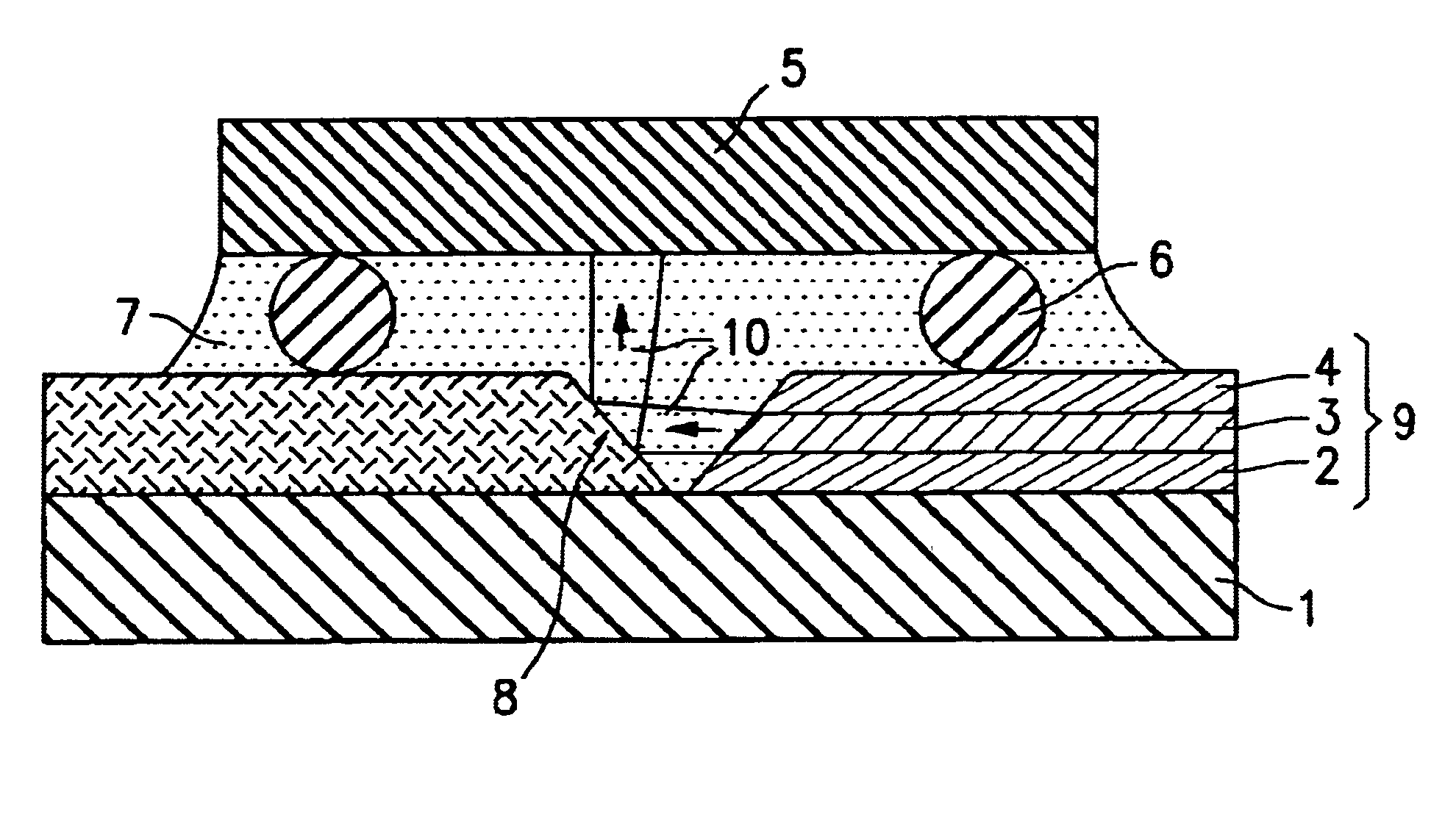
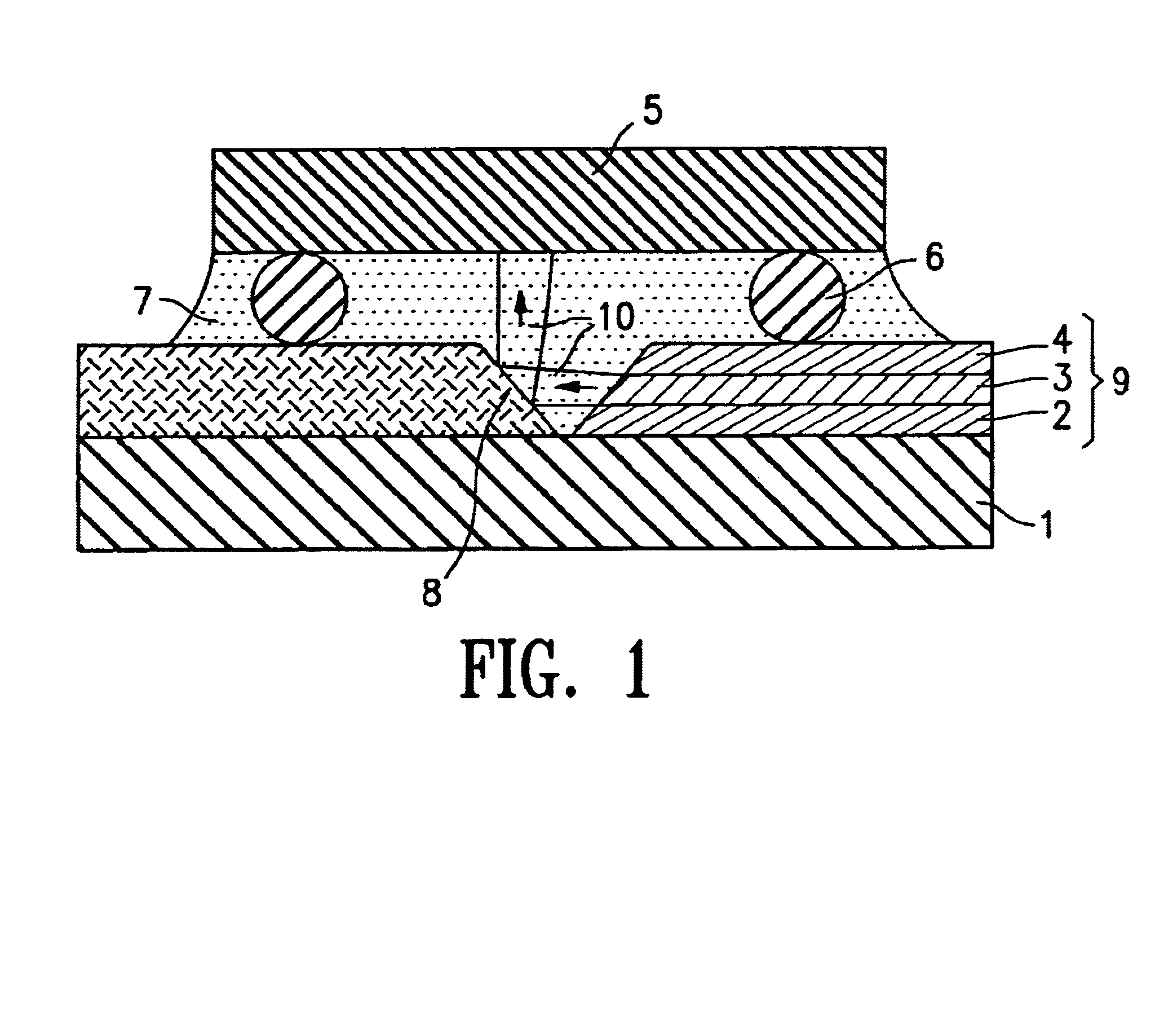
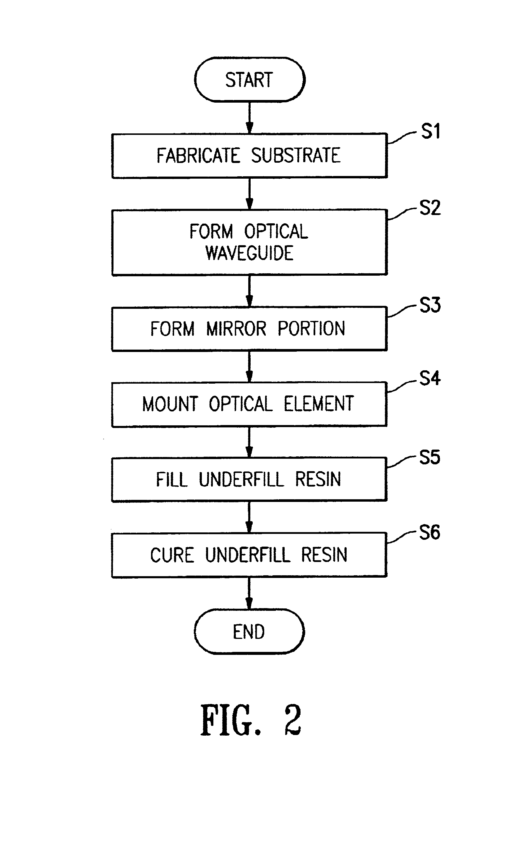
Next, with reference to FIG. 2, a specific example of the optical module embodying the invention will be described.

Firstly, at step S1, onto an alumina substrate are formed an electric wiring layer made of 2 .mu.m-thick Cu and a mounting pad used for placement of a conductor bump required to flip-chip mount an optical element 5, whereby an electric wiring substrate 1 is fabricated. The pad portion is plated with N1, then follow with 1 .mu.m-thick Au as the topmost coat.

At step S2, the substrate 1 is spin-coated with an organic solvent solution of siloxane polymer, and is then heat-treated at 85.degree. C. for 30 minutes and at 150.degree. C. for 30 minutes, whereby a 12 .mu.m-thick clad portion 2 (refractive index =1.4405 at .lambda.=1.3 .mu.m) is formed.

Then, the clad portion 2 is spin-coated with a mixed solution of siloxane polymer and tetra-n-butoxytitanium, and is then heat-treated at 85.degree. C. for 30 minutes and at 150.degree. C. for 30 minutes, whereby a 7 .mu.m-thick cor...


PUM


Abstract

An optical module comprising: an optical element flip-chip mounted on a substrate; an optical waveguide formed on the substrate and optically connected to the optical element; and underfill resin filled in between the substrate and the optical element and covering an optical junction between the optical element and the optical waveguide, wherein the underfill resin is of an electrically insulating material and has a refractive index equal to or smaller than a refractive index of a clad portion of the optical waveguide. The optical element can be flip-chip mounted with improved mechanical and electrical mounting reliability and thus satisfactory optical connection can be maintained. Further, it never occurs that light passing through the optical waveguide leaks to the underfill resin in the optical junction between the optical waveguide and the optical element.

Description

1. Field of the InventionThe present invention relates to an optical module for use in optical communication modules or the like, more particularly to an optical module obtained by flip-chip mounting a surface-operating optical element on an electric circuit substrate having an optical waveguide formed thereon and filling underfill resin in between the optical element and the substrate, wherein the electrical, optical, and mechanical mounting reliability of the optical element is successfully improved and a method for manufacturing such an optical module.2. Description of the Related ArtAs a method for mounting a semiconductor element on an electric circuit substrate, there has conventionally been known a so-called flip-chip mounting method whereby a semiconductor element is mounted via a conductor bump on an electric circuit substrate. Generally, in the flip-chip mounting, after an electric circuit substrate and a semiconductor element are electrically connected and fixed to each o...

Claims


Application Information

Patent Timeline
Patent Type & Authority Patents(United States)
IPC IPC(8): G02B6/42G02B6/12G02B6/122H01L31/02H01L31/0232H01L33/48H01S5/022
CPCG02B6/4214G02B6/4212G02B6/4232G02B2006/12061H01L2224/73204H01L2224/32225H01L2224/16225H01L2924/00H01L2924/00014H01L2224/0401
Inventor KANEKO, KATSUHIROTANAHASHI, SHIGEO
Owner KYOCERA CORP
Why Eureka
Try Eureka