Apparatus and method for optimizing the efficiency of a bypass diode in multijunction solar cells

a solar cell and bypass diode technology, applied in the field of photovoltaic cells, can solve the problems of degrading the cell, inoperable cells, and the inability of solar cells to meet the needs of more sophisticated applications

Inactive Publication Date: 2004-01-20
SOLAERO TECH CORP
View PDF14 Cites 111 Cited by
  • Summary
  • Abstract
  • Description
  • Claims
  • Application Information

AI Technical Summary

Benefits of technology

In accordance with the purpose of the invention, as embodied and broadly described herein, the invention relates to an alternative and more effective way of optimizing the efficiency of and manufacturing a bypass diode so as to create a monolithic integral bypass diode that can be manufactured with a high rate of efficiency and when operable will require less voltage than prior art devices.

Problems solved by technology

While significant progress has been made in this area, the requirement for solar cells to meet the needs of more sophisticated applications has not kept pace with demand.
This reverse biasing can degrade the cells and can ultimately render the cells inoperable.
This is a difficult device to manufacture, and charges the array assembler with a task perhaps better performed by the cell manufacturer.
However, this technique is complicated to manufacture and requires a very difficult and inefficient assembly method.
This technique has not yet proven efficient to manufacture because of the delicacy of the cells and because the technique requires the connection of the adjoining cells to be formed by the assembler of the array as opposed to the cell manufacturer.

Method used


Image

  • Apparatus and method for optimizing the efficiency of a bypass diode in multijunction solar cells
  • Apparatus and method for optimizing the efficiency of a bypass diode in multijunction solar cells
  • Apparatus and method for optimizing the efficiency of a bypass diode in multijunction solar cells

Examples


Embodiment Construction

The following describes the present invention more fully with reference to the accompanying drawings, in which a preferred embodiment of the invention is shown. The present invention may, however, be embodied in many different forms and should not be construed as being limited to the embodiment set forth herein; this embodiment is provided so that this disclosure will be thorough and complete and will fully convey the invention to those skilled in the art.

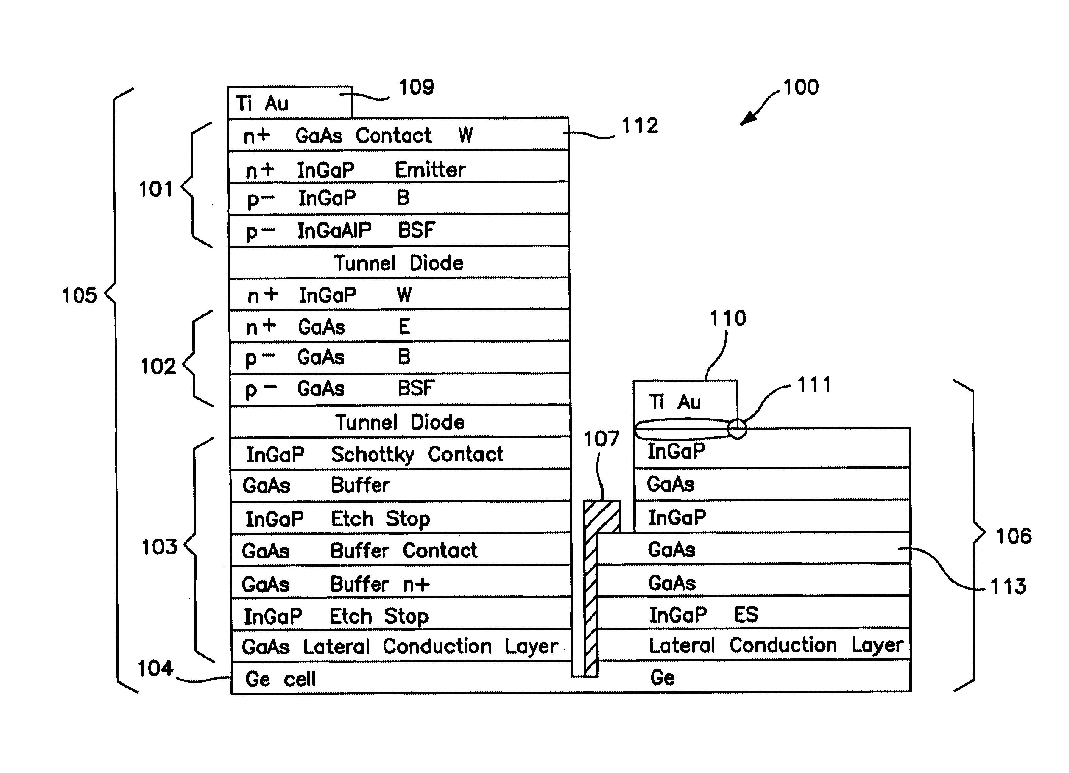
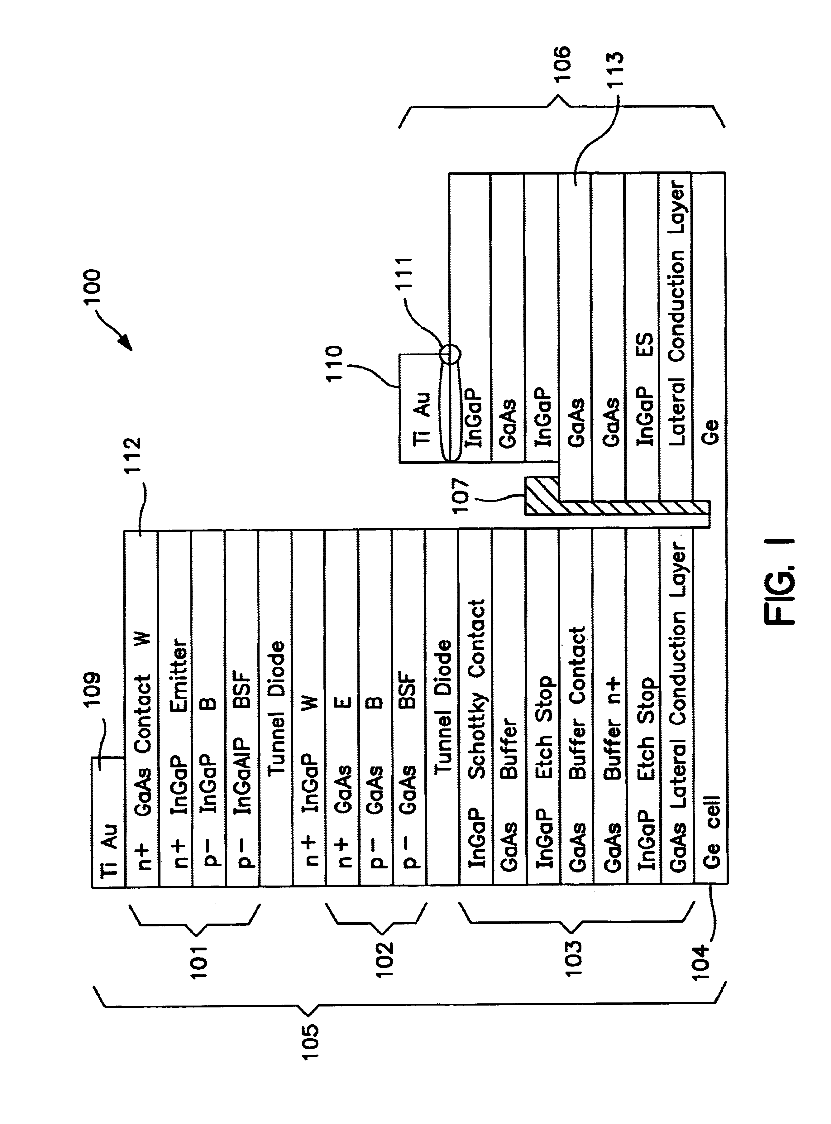
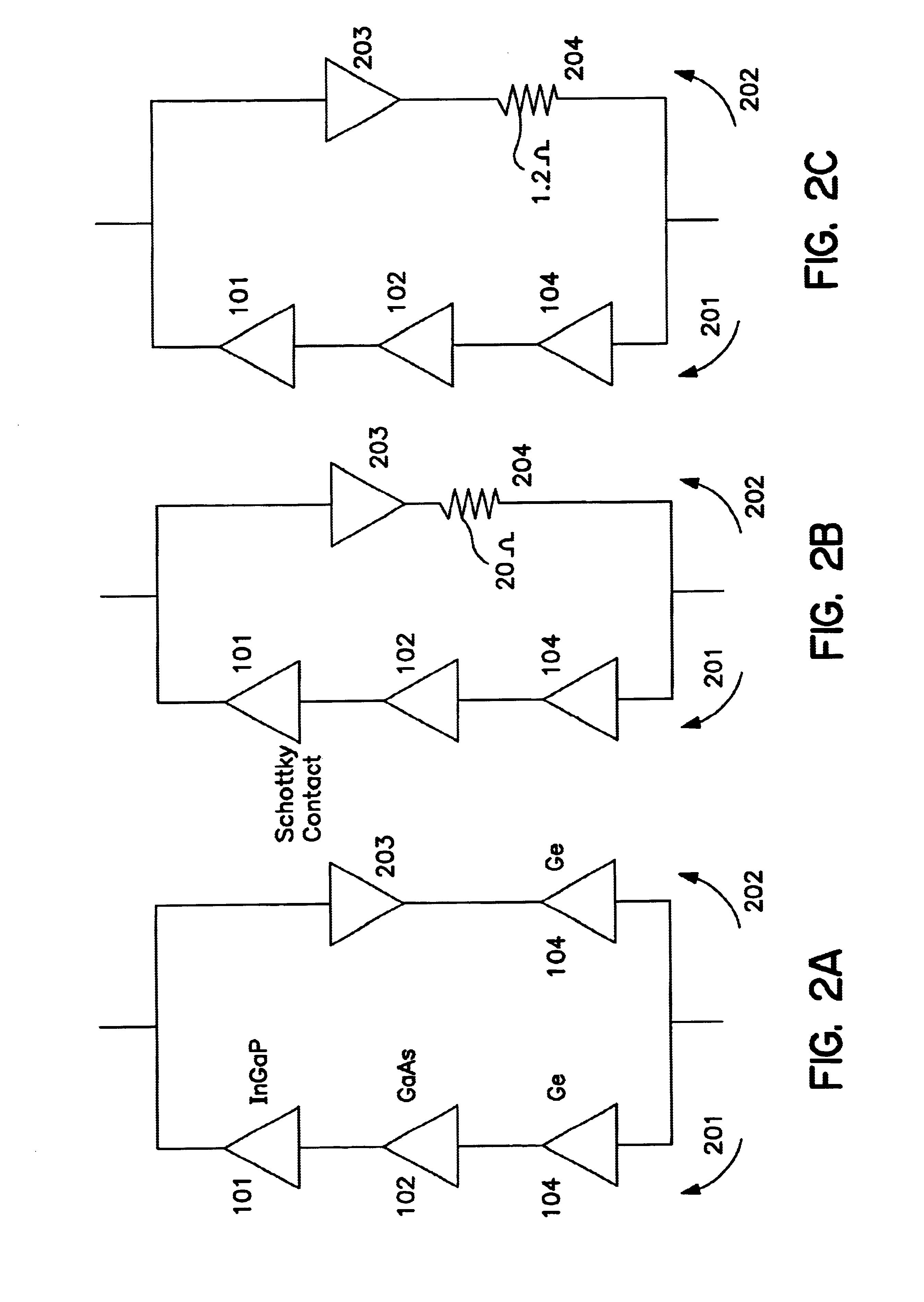
The present invention relates to a multijunction solar cell with at least one integral monolithic bypass diode. The layers comprising the solar cell are particularly chosen for their combination of efficiency and manufacturability. As discussed below, one embodiment consists of a multijunction structure with at least three junctions, with a unique modified buffer structure.

The process of manufacturing the solar cell with an integral monolithic bypass diode is comprised of five distinct steps, which are described below.

FIG. 1 is an ...


PUM


Abstract

Apparatus and Method for Optimizing the Efficiency of a Bypass Diode in Solar Cells. In a preferred embodiment, a layer of TiAu is placed in an etch in a solar cell with a contact at a doped layer of GaAs. Electric current is conducted through a diode and away from the main cell by passing through the contact point at the GaAs and traversing a lateral conduction layer. These means of activating, or "turning on" the diode, and passing the current through the circuit results in greater efficiencies than in prior art devices. The diode is created during the manufacture of the other layers of the cell and does not require additional manufacturing.

Description

The present invention relates to solar cells and methods for their fabrication, and more particularly to optimizing the efficiency of a bypass diode within solar cells.DESCRIPTION OF THE RELATED ARTPhotovoltaic cells, also called solar cells, are one of the most important new energy sources that have become available in the past several years. Considerable effort has gone into solar cell development. As a result, solar cells are currently being used in a number of commercial and consumer-oriented applications. While significant progress has been made in this area, the requirement for solar cells to meet the needs of more sophisticated applications has not kept pace with demand. Applications such as satellites used in mobile and telephone communications have dramatically increased the demand for solar cells with improved power and energy conversion characteristics.In satellite and other space related applications, the size, mass, and cost of a satellite power system is dependent on t...

Claims


Application Information

Patent Timeline
Patent Type & Authority Patents(United States)
IPC IPC(8): H01L27/142H01L31/06H01L31/072H01L31/04H01L31/00H01L31/0687H01L31/0725H01L31/0735
CPCH01L27/142H01L31/03046H01L31/0687H01L31/0725H01L31/0735H01L31/184H01L31/1852Y02E10/544Y10S136/293H01L27/1421Y02E10/547Y02P70/50
Inventor SHARPS, PAUL R.CLEVENGER, MARVIN BRADSTAN, MARK A.
Owner SOLAERO TECH CORP
Why Eureka
Try Eureka