Electrochemically generated reactants for chemical mechanical planarization

a technology of reactants and reactants, applied in the field of electrochemically generated reactants for chemical mechanical planarization, can solve the problems of increasing the overall cost of the cmp process, oxidizing the organic and metallic components of the cmp tool, and little that may be done on a more local scal

Inactive Publication Date: 2004-02-10
FULLBRITE CAPITAL PARTNERS
View PDF19 Cites 88 Cited by
  • Summary
  • Abstract
  • Description
  • Claims
  • Application Information

AI Technical Summary

Problems solved by technology

The need for frequent replenishment, of course, increases the overall cost of the CMP process and can lead to variations in the slurry composition used for, and therefore the polish rates of, successive wafers in a given lot or for successive lots.
Oxidizing agents like hydrogen peroxide also frequently oxidize organic and metallic components of CMP tools such as tubing or metallic surfaces exposed to slurry.
While all three of these methods can be effective at a macro scale across the surface of a wafer, the fact that they rely on mechanical schemes means there is little that may be done on a more local scale at various locations on the wafer surface.
However, conventional CMP processes sometimes do not proceed according to specified time periods.
Process aborts are a leading cause of such variations.
However, during an abort, the chemical activity associated with the CMP slurry may continue, resulting in a static etch of the surfaces of the wafer exposed to the slurry.
This can result in unwanted and substantial etch attack of various structures on the wafer.

Method used


Image

  • Electrochemically generated reactants for chemical mechanical planarization
  • Electrochemically generated reactants for chemical mechanical planarization
  • Electrochemically generated reactants for chemical mechanical planarization

Examples


Embodiment Construction

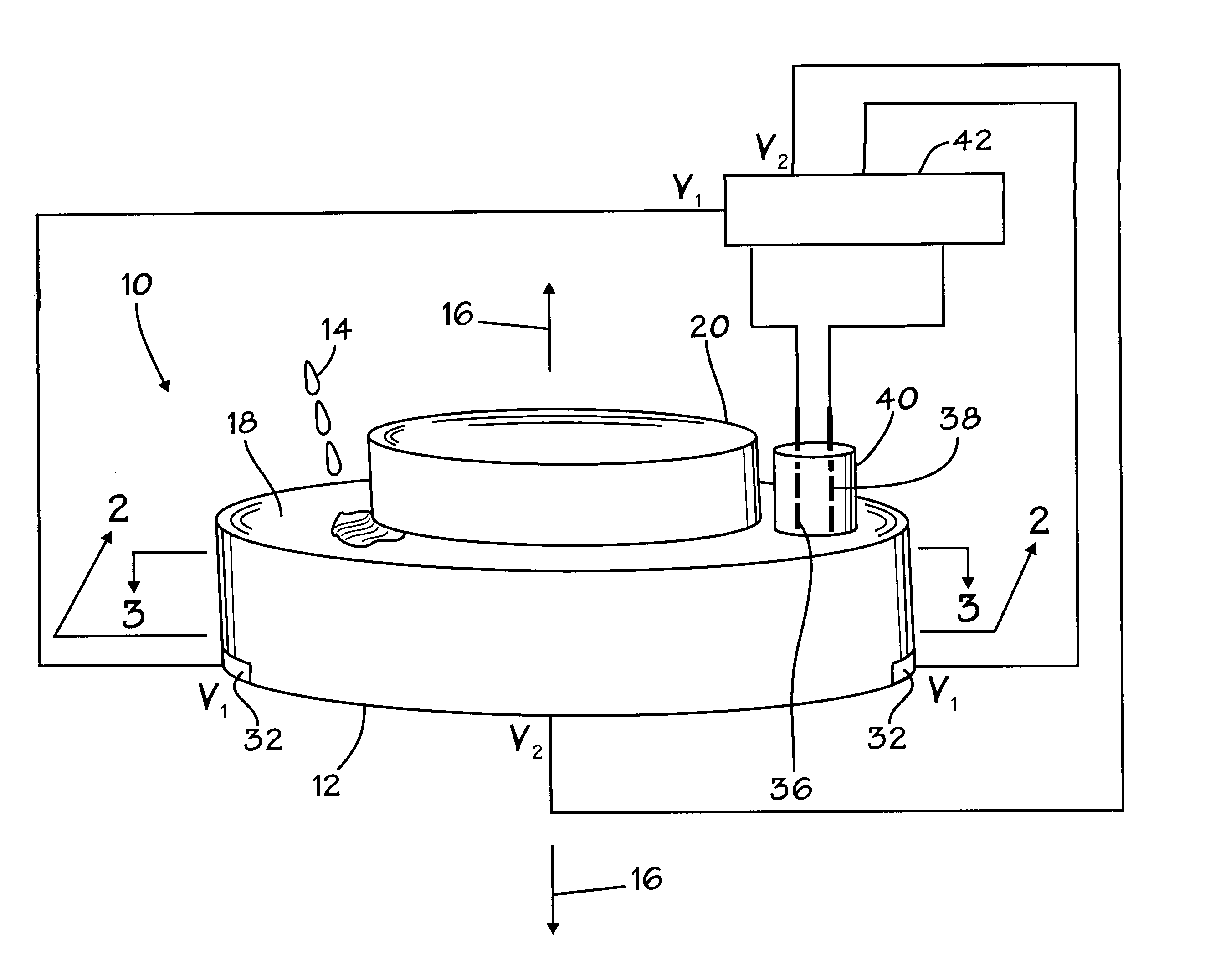
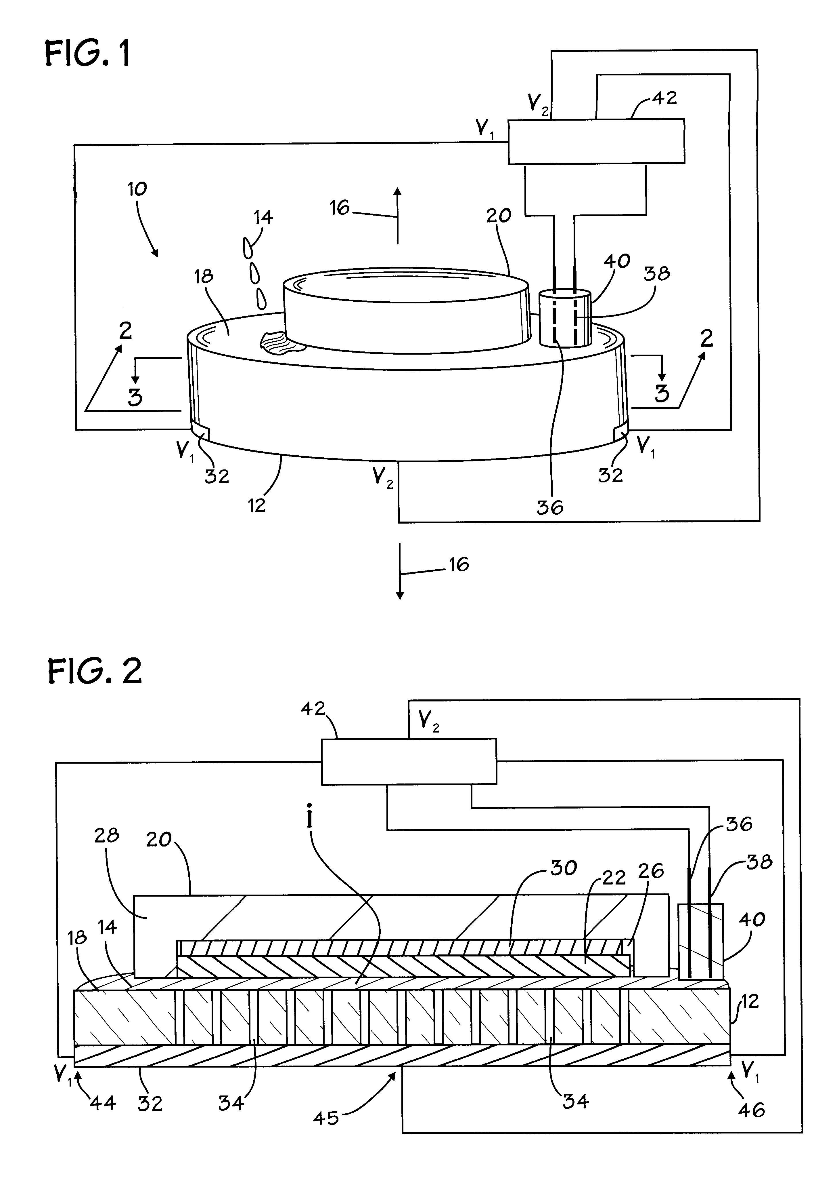
In the drawings described below, reference numerals are generally repeated where identical elements appear in more than one figure. Turning now to the drawings, and in particular to FIG. 1, therein is shown a pictorial view of an exemplary embodiment of a chemical mechanical polishing system 10 (hereinafter CMP system 10) that utilizes electrochemistry for generation of chemical species useful in CMP in accordance with the present invention. For better understanding, FIG. 1 should be viewed in conjunction with FIG. 2, which is a cross-sectional view of FIG. 1 taken at section 2--2. The CMP system 10 includes a member or table 12 that is operable to receive a quantity of an electrically conducting solution 14 dispensed from a reservoir or other dispensing system (not shown). The table 12 maybe motorized and therefore operable to rotate about an axis 16. An upper surface 18 of the table 12 functions as a polish pad surface and will typically be composed of a compliant material such as...


PUM

PropertyMeasurementUnit
electrochemical potentialaaaaaaaaaa
centrifugal forceaaaaaaaaaa
period of timeaaaaaaaaaa

Abstract

Various methods and apparatus for polishing semiconductor workpieces using electrochemically generated species are disclosed. In one aspect, a method of processing is provided that includes contacting a semiconductor workpiece to a solution, electrochemically generating a chemical species in the solution, and polishing the semiconductor workpiece with the aid of the solution.

Description

1. Field of the InventionThis invention relates generally to semiconductor processing, and more particularly to chemical mechanical polishing and methods of performing the same.2. Description of the Related ArtConventional chemical mechanical planarization or polishing ("CMP") processes involve the planarization of a surface of a wafer or workpiece through the use of an abrasive slurry and various rinses and solvents. Material removal from the workpiece surface is through a combination of abrasive action and chemical reaction. In many processes, a quantity of abrasive slurry is introduced onto a polish pad of the CMP tool and distributed across the surface thereof by means of centrifugal force. Thereafter, one or more wafers are brought into sliding contact with the polish pad for a select period of time.Conventional slurries normally contain several components, such as one or more types of abrasive particles, a stabilizer that is designed to keep the abrasive particles from going i...

Claims


Application Information

Patent Timeline
Patent Type & Authority Patents(United States)
IPC IPC(8): B24B37/04H01L21/70H01L21/02H01L21/768H01L21/321B23H5/08
CPCB23H5/08B24B37/042B24B37/046H01L21/32125H01L21/7684
Inventor LANSFORD, CHRISTOPHER H.LANSFORD, JEREMY S.
Owner FULLBRITE CAPITAL PARTNERS
Why Eureka
Try Eureka