Semiconductor display device and driving circuit therefor

a technology of display device and semiconductor, applied in semiconductor devices, instruments, electrical devices, etc., can solve problems such as easy damage of tft, unwanted radiation due to clock signals, and failure to operate type

Inactive Publication Date: 2004-03-30
SEMICON ENERGY LAB CO LTD
View PDF29 Cites 45 Cited by
  • Summary
  • Abstract
  • Description
  • Claims
  • Application Information

AI Technical Summary

Problems solved by technology

Further, unwanted radiation due to the clock signal is a problem of the set.
There is a problem in that the n-channel-type TFT which constitutes the analog switch does not operate with a .+-.5 V voltage amplitude level image signal and sampling does not occur, when sampling is attempted using a timing signal with the same .+-.5 V voltage amplitude level, which does not include a margin.
Further, a p-channel type TFT does not operate for the same reason.
In order to operate the shift register circuit at higher speed, it is necessary to either make the shift register circuit power supply voltage large, or to shorten the channel length, because there is a limit to the extent of the TFT mobility.
However, if power supply voltage for the shift register circuit is made higher, and the channel length is made shorter, the TFT is easily damaged by punch through and hot electrons caused by the short channel effect.
In addition, if the voltage amplitude level of the clock signal applied to the source is reduced to a level that will not damage the TFT due to punch through or hot electrons caused by a short channel effect of the shift register circuit TFT, and if the TFT channel length is made shorter, then the TFT can not be manufactured due to limits in the design of TFTs with short channels.
Therefore the shift register circuit TFT is easily damaged.
There is a solution path for the above problems by using a liquid crystal display device structured with a LCD material that can be driven with a relatively low voltage, smaller than 3 V. However, the reliability is low because the liquid crystal used has a voltage holding rate that is low, current leaks due to the voltage applied to the liquid crystals, and the liquid crystals easily deteriorate.
However, with the circuit structure of Prior Art B, if the voltage amplitude level of the clock signal, input from external to the source signal line side driving circuit, is increased to a high voltage, to a voltage amplitude level at which the shift register circuit can operate at high-speed, it is difficult to suppress the voltage amplitude level of the clock signal, input from external to the source signal line side driving circuit, to a level at which unwanted radiation does not become a problem.
Further, the higher the voltage amplitude level of the clock signal input from external to the source signal line side driving circuit becomes, the larger the power consumption, which is not desirable.
There is a solution path for the above problems by using a liquid crystal display device structured with a LCD material that can be driven with a relatively low voltage, smaller than 3 V. However, the reliability is low because the liquid crystal used has a voltage holding rate that is low, current leaks due to the voltage applied to the liquid crystals, and the liquid crystals easily deteriorate.
It is self-evident that the Prior Art C possesses the drawbacks of both Prior Art A and Prior Art B. If the liquid crystals are driven in the saturation state, the TFT of the shift register circuit is easily damaged due to punch through and hot electrons resulting from the short channel effect, so there is a problem that the channel length cannot be shortened and therefore high-speed operation is not possible.
Therefore this cannot be suppressed enough to avoid the problems of unwanted radiation and power consumption.
There is a solution path for the above problems by using a liquid crystal display device structured with a LCD material that can be driven with a relatively low voltage, smaller than 3 V. However, the reliability is low because the liquid crystal used has a voltage holding rate that is low, current leaks due to the voltage applied to the liquid crystals, and the liquid crystals easily deteriorate.
The TFT channel length on the shift register circuit is longer on the gate signal line side driving circuit than on the source signal line side driving circuit, which has an operating speed slower than the source signal line side driving circuit, and it is difficult for damage to occur from punch through or hot electrons due to the short channel effect.
There is a solution path for the above problems by using a liquid crystal display device structured with a LCD material that can be driven with a relatively low voltage, smaller than 3 V. However, the reliability is low because the liquid crystal used has a voltage holding rate that is low, current leaks due to the voltage applied to the liquid crystals, and the liquid crystals easily deteriorate.
It is self-evident that the Prior Art E possesses the same drawbacks as Prior Art B. With Prior Art B, if the input clock signal is given a voltage amplitude level at which high-speed operation of the shift register circuit is possible, then it is difficult to reduce it to a degree at which unwanted radiation will not become a problem.
In addition, as stated above, there is a problem of not being capable of suppressing the power consumption.
There is a solution path for the above problems by using a liquid crystal display device structured with a LCD material that can be driven with a relatively low voltage, smaller than 3 V. However, the reliability is low because the liquid crystal used has a voltage holding rate that is low, current leaks due to the voltage applied to the liquid crystals, and the liquid crystals easily deteriorate.
It is self-evident that the Prior Art F possesses the same drawbacks as Prior Art C. If all of the pixel TFTs are to be reliably driven, the channel length cannot be shortened because the shift register circuit TFT is easily damaged by punch through and hot electrons due to the short channel effect, and therefore there is a problem of not being cable of operating at high-speed.
There is a solution path for the above problems by using a liquid crystal display device structured with a LCD material that can be driven with a relatively low voltage, smaller than 3 V. However, the reliability is low because the liquid crystal used has a voltage holding rate that is low, current leaks due to the voltage applied to the liquid crystals, and the liquid crystals easily deteriorate.
A liquid crystal display device which can be driven at a relatively low voltage below 3V, the voltage holding rate is low, there is a current leak due to the voltage applied to the liquid crystals, and the liquid crystals easily deteriorate, so the reliability is low.
However, if the liquid crystals are driven to a saturation state by a conventional source signal line side driving circuit when a liquid crystal display device driven by a relatively high voltage is used, then the shift register circuit TFT is easily damaged by punch through and hot electrons due to the short channel effect.
However, if the power consumption and the unwanted radiation with a conventional source signal line side driving circuit are suppressed, high-speed operation of the shift register circuit is difficult, and the demands accompanying large screens cannot be met.
Similarly for the gate signal line side driving circuit, if all of the pixel TFTs are to be reliably driven, the shift register circuit TFT is easily damaged by punch through and hot electrons due to the short channel effect.
If the power consumption and the unwanted radiation are suppressed, then high-speed operation of the shift register circuit is difficult, and the demands accompanying large screens cannot be met.

Method used


Image

  • Semiconductor display device and driving circuit therefor
  • Semiconductor display device and driving circuit therefor
  • Semiconductor display device and driving circuit therefor

Examples


embodiment 1

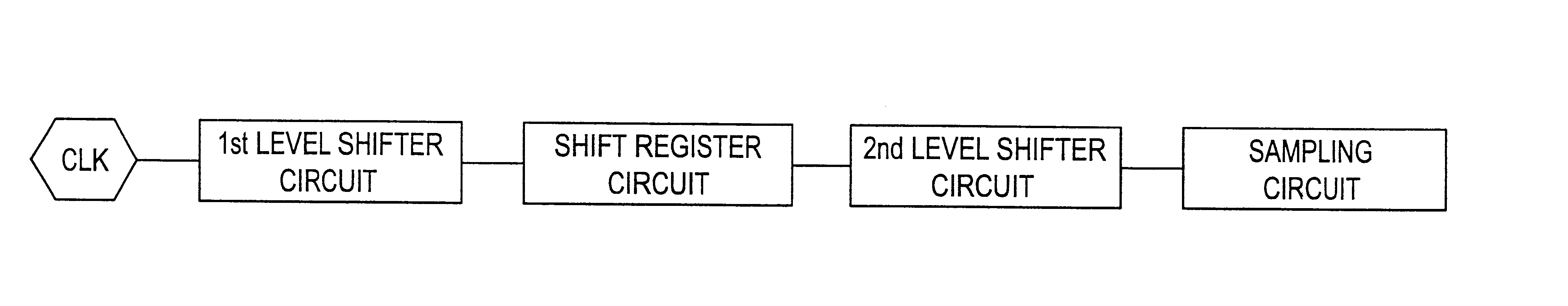
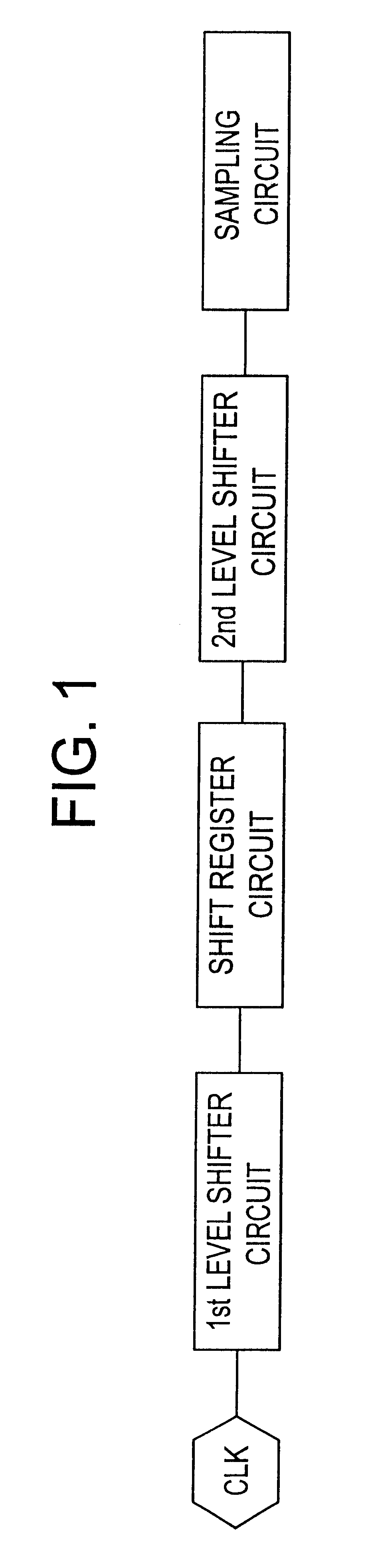
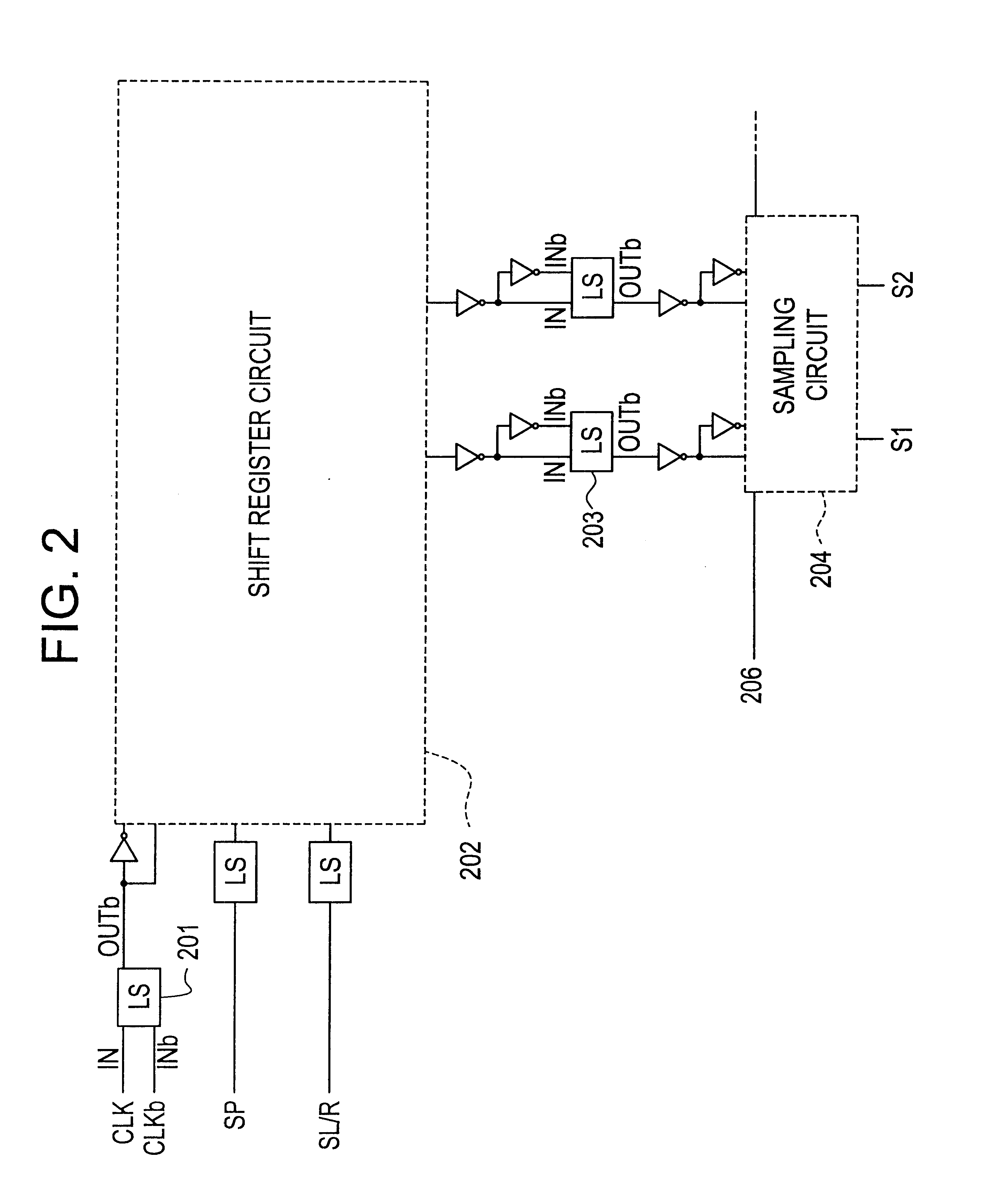
The voltage amplitude level of the clock signal input to the first level shifter circuit is increased (made higher voltage) by the first level shifter circuit, from 2.5 V to 5 V in Embodiment 1, and the result is input to the shift register circuit.

The voltage amplitude level of the clock signal input to the shift register circuit is required to be a voltage amplitude level that is within the range in which the shift register circuit can operate. The shift register circuit can operate at 5 V in Embodiment 1. For example, in order to operate the shift register circuit of the source signal line side driving circuit at 12.5 MHz or greater in Embodiment 1, when configured by a TFT with a 2 .mu.m channel length, it is necessary for the voltage amplitude level of the clock signal input to the shift register circuit to be 4 V or greater. The voltage amplitude level is increased to 5 V in Embodiment 1, but the voltage amplitude level is not limited to this number for the present invention. ...

embodiment 2

Another example of a source signal line side driving circuit using the structure of the present invention, in which, by arranging level shifter circuits before and after a shift register circuit, the voltage amplitude level of a signal is increased in two stages, before and after the shift register circuit, is shown in Embodiment 2.

Next, a block diagram of the source signal line side driving circuit of Embodiment 2 is shown in FIG. 7. In Embodiment 2 a liquid crystal with a saturation voltage of 6 V is used. A clock signal CLK, with a voltage amplitude level of 3 V and from external to the is source signal line side driving circuit, is input to a first level shifter circuit of the source signal line side driving circuit. The voltage amplitude level of the clock signal input to the first level shifter circuit needs to be as low as possible, within the range in which the first level shifter circuit can operate, in order to suppress unwanted radiation to an extent where it does not bec...

embodiment 3

Another example of a source signal line side driving circuit using the structure of the present invention, in which, by arranging level shifter circuits before and after a shift register circuit, the voltage amplitude level of a signal is increased in two stages, before and after the shift register circuit, is shown in Embodiment 3.

Next, a block diagram of the source signal line side driving circuit of Embodiment 3 is shown in FIG. 8. In Embodiment 3 a liquid crystal with a saturation voltage of 7 V is used. A clock signal CLK, with a voltage amplitude level of 5 V and from external to the source signal line side driving circuit, is input to a first level shifter circuit of the source signal line side driving circuit. The voltage amplitude level of the clock signal input to the first level shifter circuit needs to be as low as possible, within the range in which the first level shifter circuit can operate, in order to suppress unwanted radiation to an extent where it does not become...


PUM


Abstract

A semiconductor display device with low power consumption, low electromagnetic noise, and low unwanted radiation is provided. In a peripheral driving circuit, a clock signal with a voltage level increased by a level shifter circuit is input to a shift register circuit. Then a timing signal from the shift register circuit is input to a level shifter circuit, and the voltage level is thus raised in two stages.

Description

1. Field of the InventionThe present invention relates to a semiconductor display device. More specifically, it relates to a semiconductor display device which performs image display by driving pixel TFTs arranged in a matrix state, and to a semiconductor display device driving circuit. In addition, it relates to electronic equipment using such semiconductor display devices.2. Description of the Related ArtRecently there has been rapid development in techniques of manufacturing semiconductor display devices, for example a thin film transistor (TFT), formed from semiconductor thin films on an inexpensive glass substrate. The reason for this is because the demand for active matrix type liquid crystal display devices has risen.A TFT is placed in each of the several hundreds of thousands to several millions of pixel regions arranged in a matrix state on an active matrix type liquid crystal display device. The electric charge entering and exiting every pixel electrode is controlled by th...

Claims


Application Information

Patent Timeline
Patent Type & Authority Patents(United States)
IPC IPC(8): G09G3/36G09G3/30
CPCG09G3/30G09G3/3677G09G3/3688G09G3/3674G09G3/3685G09G2300/0809G09G2300/0842G09G2310/0267G09G2310/027G09G2310/0275G09G2310/0286G09G2310/0289G09G2330/02H01L27/12H01L27/1214H01L27/13H01L29/4908H01L29/78621H01L29/78627H01L27/1255H01L27/1277
Inventor YAMAZAKI, SHUNPEIKOYAMA, JUN
Owner SEMICON ENERGY LAB CO LTD
Why Eureka
Try Eureka