Method for automatic organization of microstructures or nanostructures and related device obtained

a technology of microstructures and nanostructures, applied in the direction of polycrystalline material growth, crystal growth process, chemically reactive gases, etc., can solve the problems of system unusability, limiting the choice of materials from which to make the nanostructure, and none of these techniques appear to make auto-organization of nanostructures of nanometric size feasible with a good size uniformity

Inactive Publication Date: 2004-04-20
COMMISSARIAT A LENERGIE ATOMIQUE ET AUX ENERGIES ALTERNATIVES +1
View PDF5 Cites 25 Cited by
  • Summary
  • Abstract
  • Description
  • Claims
  • Application Information

AI Technical Summary

Benefits of technology

The intermediate layer in the invention prevents any contamination of nanostructures by the substrate. Its function is firstly to facilitate putting nanostructures into order on the substrate and secondly to isolate nanostructures from the substrate.
Step a) may include bringing two wafers of crystalline material into contact such that the crystalline lattices formed on the faces of the wafers brought into contact are offset by an angle enabling the formation of a network of crystalline defects within a crystalline zone close to the interface of the two wafers, one of the wafers then being thinned to reveal said surface with a stress field or topology associated with a stress field.
The intermediate layer may be composed of a stack of sub-layers. According to a first variant, the sub-layers are composed of the same material but have different roughnesses. According to a second variant, the sub-layers are composed of different materials, for example SiO.sub.2 and Si.sub.3 N.sub.4. According to yet another variant, the stack of sub-layers includes sub-layers with stress values with opposed signs. This can give an amplification effect in sub-layers making up the intermediate layer.

Problems solved by technology

None of these techniques appears to make auto-organisation of nanostructures of nanometric size feasible with a good size uniformity.
There are several problems inherent to these known processes.
A first problem is due to the fact that the nanostructures are in direct contact with the support substrate, even if the space between the nanostructures may be of different nature, and particularly different electrical nature, after appropriate treatment such as heat treatment.
This type of leak makes the system unusable for controlling the transport of an electron from one nanostructure to another.
A second problem is the result of the fact that processes according to prior art require the generation of a stress field in the substrate, which limits the choice of the material from which the nanostructures are made.
A third problem relates to optimisation of nanostructure devices.

Method used


Image

  • Method for automatic organization of microstructures or nanostructures and related device obtained
  • Method for automatic organization of microstructures or nanostructures and related device obtained
  • Method for automatic organization of microstructures or nanostructures and related device obtained

Examples


Embodiment Construction

The following part of the description relates to making nanostructures on a support.

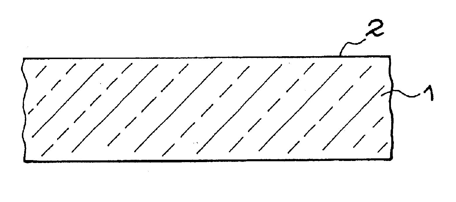
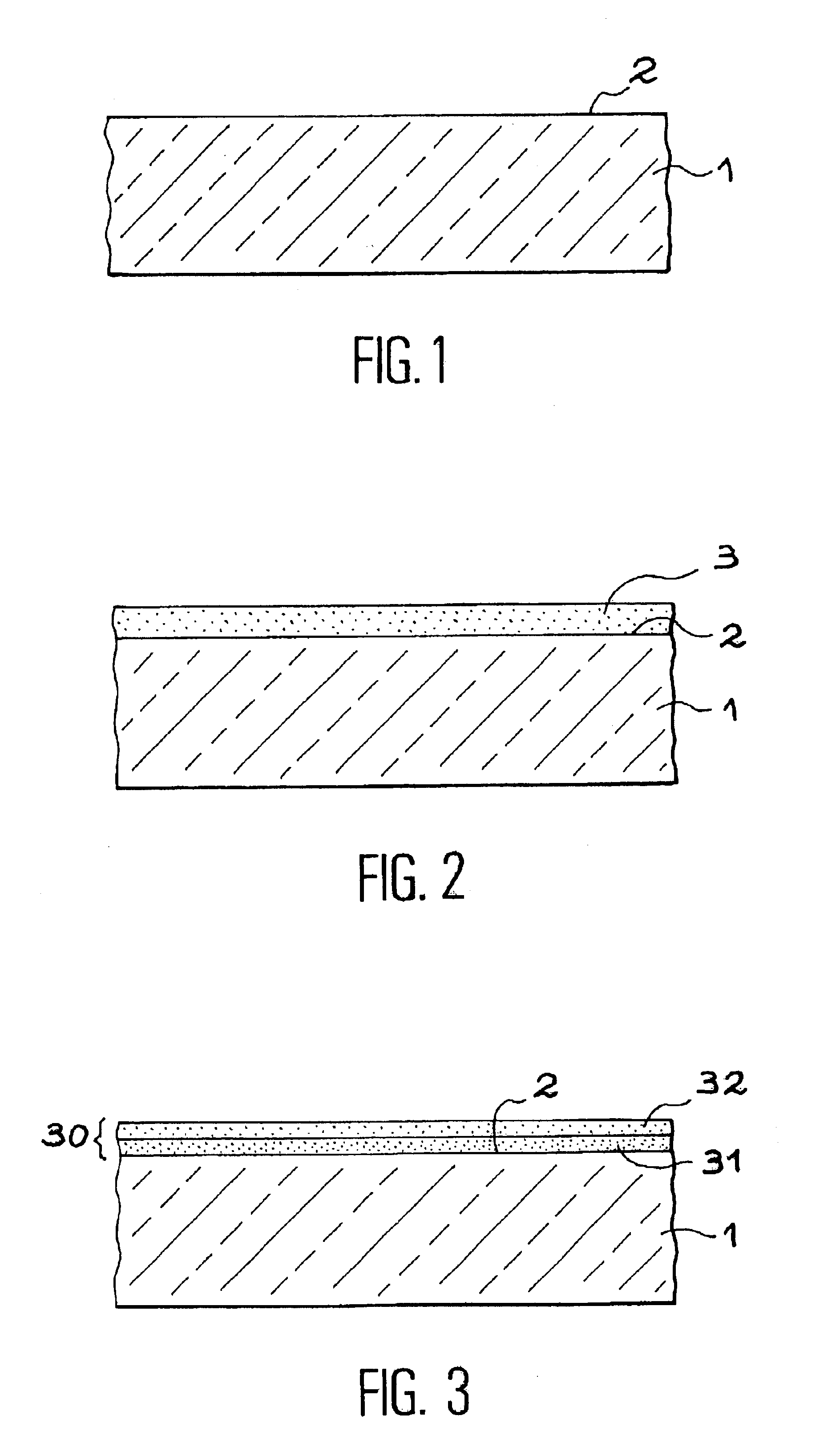
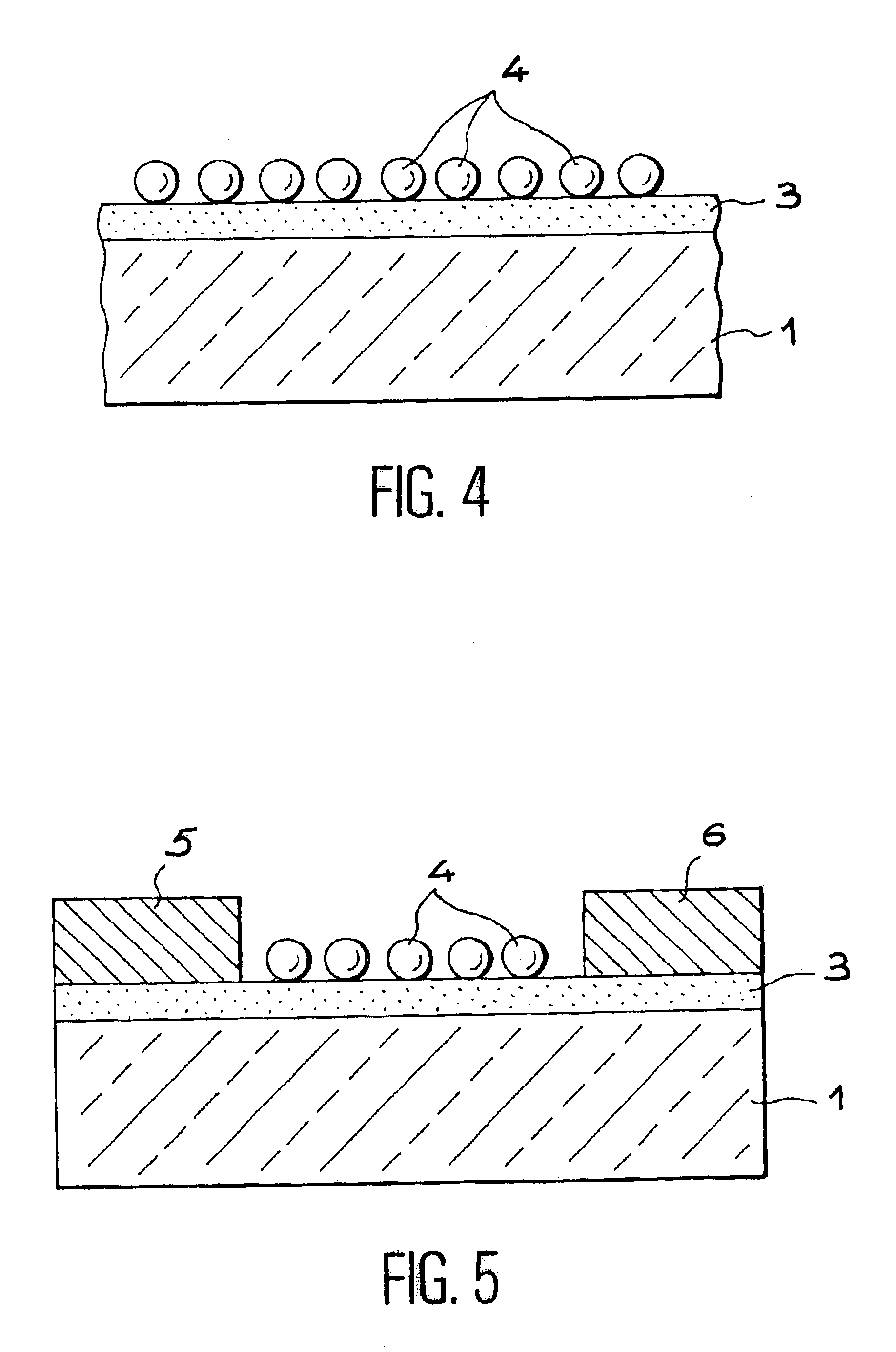
The device according to the invention includes a support composed of a substrate and a layer of material called the intermediate layer on which the nanostructures are deposited. For example, the substrate may be of the type described in document FR-A-2 766 620. FIG. 1 shows such a substrate, reference 1, with a surface 2 with a stress field.

The surface 2 of the substrate 1 is treated such that the intermediate layer formed on it is covering, uniform and homogeneous. For a substrate made of silicon, this treatment may be based on chemistry based on dilute HCl including ozone according to a known technique in microelectronics.

FIG. 2 shows the substrate 1 in FIG. 1 supporting an intermediate layer 3 formed from the treated surface 2. The intermediate layer 3 may be deposited on the surface 2 by a PVD technique or a CVD technique or a combination of the PVD and CVD techniques. If the substrate 1 is made ...


PUM

PropertyMeasurementUnit
temperatureaaaaaaaaaa
thicknessaaaaaaaaaa
resistivityaaaaaaaaaa

Abstract

The invention relates to a device comprising microstructures or nanostructures on a support, characterized in that the support comprises:a) a substrate (1) comprising at least one part composed of a crystalline material, this part having a surface (2) with a stress field or a topology associated with a stress field, the stress field being associated with dislocations,b) an intermediate layer (3) bonded to the surface (2), and having a thickness and / or composition and / or a surface state enabling transmission of said stress field through this layer as far as its free face that supports microstructures or nanostructures (4).

Description

The invention relates to an auto-organisation process for microstructures or nanostructures in a two-dimensional or three-dimensional lattice. It also relates to a device with auto-organised microstructures or nanostructures.These microstructures or nanostructures are designed for making electronic, optical, opto-electronic or magnetic devices, and particularly Coulomb blocking devices using quantum dots.STATE OF PRIOR ARTIt is known that a microstructure or nanostructure arrangement on a surface can be determined using conventional photolithoetching methods. For example, a continuous layer of material chosen as a constituent of microstructures or nanostructures can be deposited on a surface. This may be a layer of silicon deposited by LPCVD. This layer is covered by a photosensitive film. After this film has been exposed, the geometries are recorded and are then transferred to the subjacent material. The state of the art is thus capable of defining nanostructures of the order of 20...

Claims


Application Information

Patent Timeline
Patent Type & Authority Patents(United States)
IPC IPC(8): C23C16/02C23C14/02C30B25/02
CPCC23C14/024C23C16/0272C30B25/02C30B29/605
Inventor SEMERIA, MARIE-NOELLEMUR, PIERREFOURNEL, FRANCKMORICEAU, HUBERTEYMERY, HUBERTMAGNEA, NOELBARON, THIERRYMARTIN, FRAN.CEDILLA.OIS
Owner COMMISSARIAT A LENERGIE ATOMIQUE ET AUX ENERGIES ALTERNATIVES
Why Eureka
Try Eureka