Thin film writer with multiplayer write gap

a write gap and film writer technology, applied in the field of thin film writers with multiplayer write gaps, can solve the problems of increasing operating temperature and conductor resistance, increasing so as to improve the control of the thickness of the write gap, reduce the roughness of the surface of the coil, and improve the control of the write gap thickness.

Inactive Publication Date: 2004-04-20
WESTERN DIGITAL TECH INC
View PDF7 Cites 163 Cited by
  • Summary
  • Abstract
  • Description
  • Claims
  • Application Information

AI Technical Summary

Benefits of technology

An advantage of a write head with a multilayer write gap is that it allows better control of write gap thickness. As such, loss of write gap thickness can be compensated for by deposition of the second write gap layer, or by deposition of the third write gap layer. Furthermore, the thickness of a subsequently deposited write gap layer / layers may be selected during processing to compensate for unintended loss of first or second write gap layers occurring during write head fabrication. As such write head performance and yield may be better controlled.
In addition, embodiments having the first write gap layer can inhibit oxidation of the planarized lower pole tip during conductor fabrication, which is of particular importance when the lower pole tip is formed of high moment materials more susceptible to corrosion.
Embodiments having the second write gap layer can inhibit corrosion or oxidation of the conductor turns that can form during the curing process used to form the stack insulation. The second write gap layer also may serve as a corrosion protection layer for the lower pole tip during the stack insulation curing process, particularly in embodiments not employing the first write gap layer. Also, the second write gap layer can reduce the roughness of the surface of the coil turns, which may reduce the roughness of the top surface of the stack insulation resulting in improved material properties of the upper pole structure.
Embodiments having the third write gap layer can improve the properties of overlying high moment materials. Moreover, the third write gap layer can reduce magneto-strictive effects and delamination of the write head structures. Also, the third write gap may provide added protection of outlying stack insulation and conductor turns during ion milling processes.
Further, embodiments having the second and / or third write gap layer allow stack insulation height to be reduced by serving as additional protection against shorting of the conductor turns. As such, shorting due to pin holes or other stack insulation non-uniformity may be inhibited in reduced stack height writers.

Problems solved by technology

Some high moment materials, for example, are more readily subject to corrosion if exposed to air.
In addition, the magnetic properties of high moment materials can degrade if deposited over sloped surfaces.
One impediment to optimum performance observed by the present inventors is that conductors can corrode or oxidize within the stack insulation, thus increasing operating temperature and conductor resistance.
This can occur during the insulation stack curing process and cause a shell of oxidation to form on the surface of the conductor.
Another problem associated with conventional windings identified by the present inventors is that pin holes in the stack insulation can cause shorting to the upper pole structure.
Also, etching or milling to define the upper pole structure from high B.sub.sat, or other sputtered material, can result in milling through outlying portions of the stack insulation and into the conductor winding, thus reducing conductor winding performance.
A further drawback with conventional write heads noted by the present inventors is that thermal expansion of cured photoresist stack insulation can degrade write head performance.
Further, thermal expansion can ultimately lead to delamination of stack insulation and the upper pole structure.

Method used


Image

  • Thin film writer with multiplayer write gap
  • Thin film writer with multiplayer write gap
  • Thin film writer with multiplayer write gap

Examples


Embodiment Construction

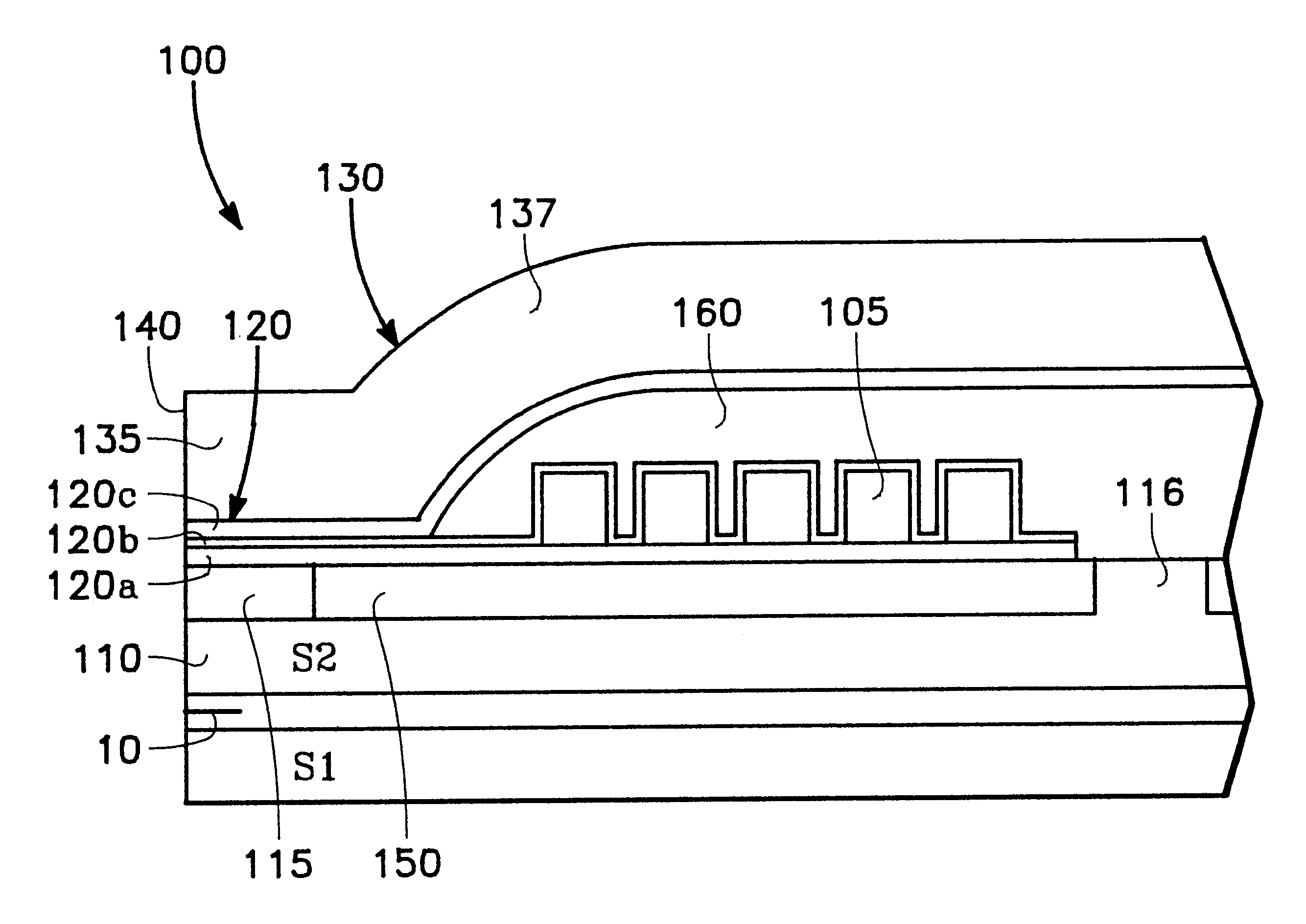
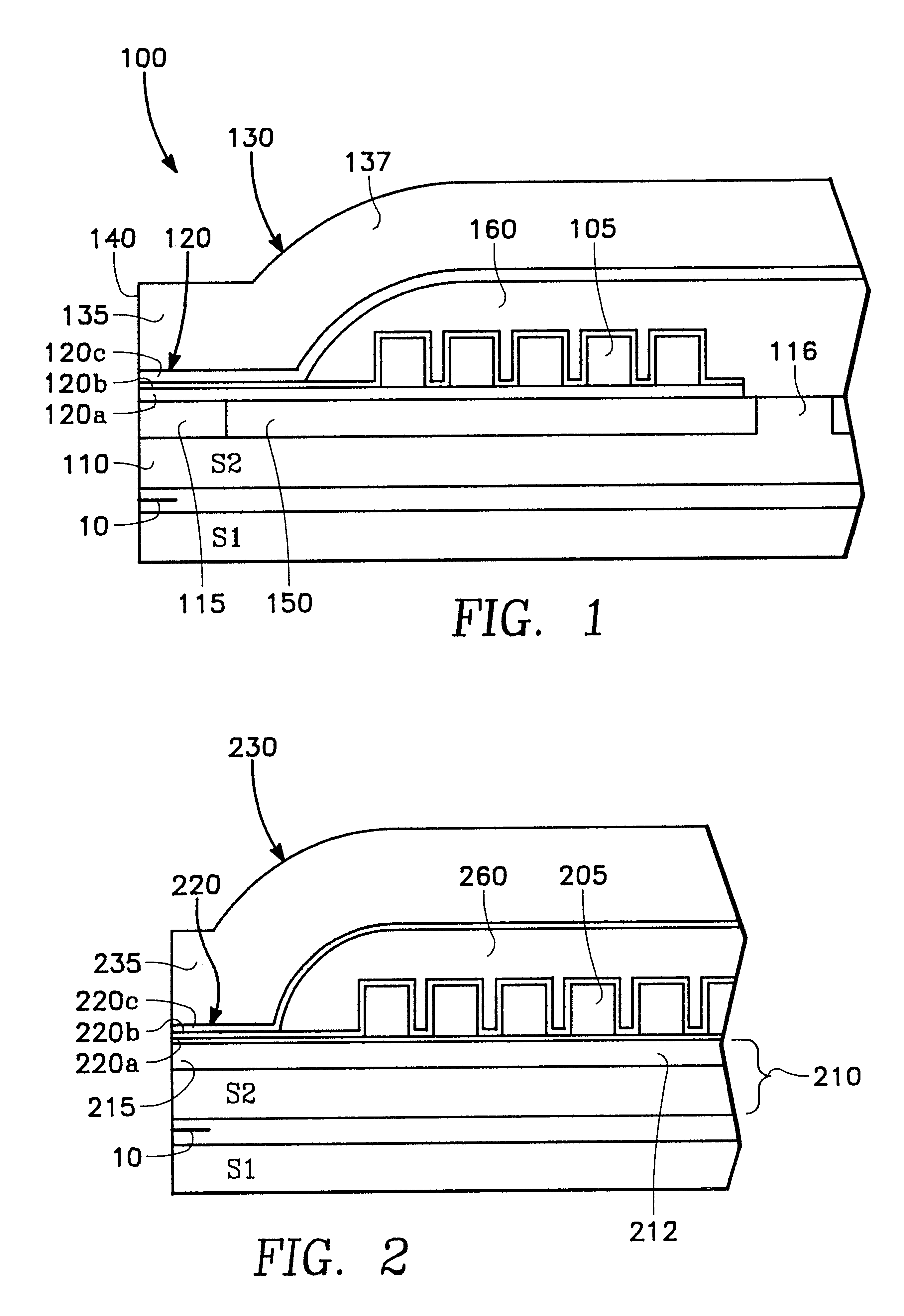
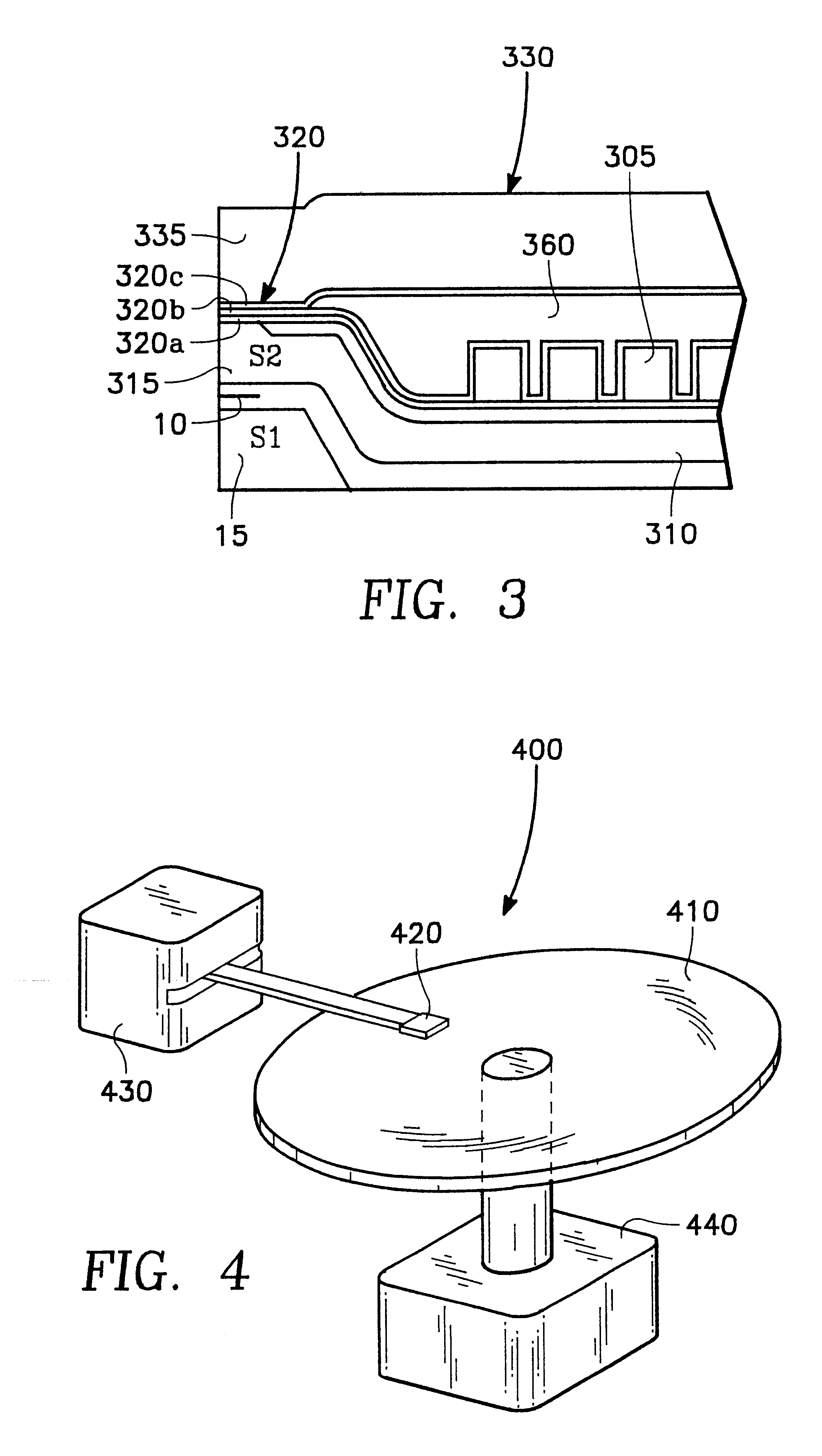
FIG. 1 shows a partial cross-sectional side view of a thin film write head 100 in accordance with a preferred embodiment of the present invention. Such an embodiment can be formed over a substrate and over a previously formed read head 10 in a merged head or other configuration known in the art.

The embodiment of FIG. 1 has lower and upper pole structures 110 and 130. The lower pole structure 110 has a pedestal pole tip portion 115 which may be a separate structure, or may be integrally formed from the material of the lower pole structure 110. The upper pole structure 130 has an upper pole tip portion 135 at an air bearing surface 140 and a yoke portion 137.

The lower pole tip 115 opposes the upper pole tip 135 across a write gap 120. Conductor turns 105 form a winding which generates magnetic flux in poles 110 and 130, which is supplied across the right gap 120 at the air bearing surface 140 to write to magnetic media (not shown).

In this preferred embodiment, the write gap 120 is for...


PUM

PropertyMeasurementUnit
thicknessaaaaaaaaaa
thicknessaaaaaaaaaa
pole structureaaaaaaaaaa

Abstract

Embodiments in accordance with the thin film write head of the present invention have a lower pole structure, an upper pole structure, and a multilayer write gap extending from an air bearing surface between the upper and lower pole structures. In preferred embodiments, the write gap comprises at least two of: (a) a first layer covering a lower pole tip portion of the lower pole structure, (b) a second layer covering turns of a semiconductor winding, or (c) a third layer covering a winding insulation stack. In more preferred embodiments, the write gap is formed of the first, the second, and the third write gap layers. An advantage of a write head with a multilayer write gap is that it allows better control of write gap thickness. As such, loss of write gap thickness can be compensated for by deposition of the second write gap layers, or by deposition of the third write gap layer. Some embodiments have one or more additional advantages in providing increased corrosion prevention, improving the integrity of conductor insulation, and / or improving the top pole magnetic material characteristics.

Description

BACKGROUNDData is stored on magnetic media by writing on the magnetic media using a write head. Magnetic media can be formed in any number of ways, such as tape, floppy diskette, and hard disk. Writing involves storing a data bit by utilizing magnetic flux to set the magnetic moment of a particular area on the magnetic media. The state of the magnetic moment is later read, using a read head, to retrieve the stored information.Data density is an important measured write head performance. Data density is determined by the amount of data stored on an area of magnetic media and depends on how much area must be allocated to each bit. Data on magnetic media is often stored in a line or track. Magnetic media often have multiple tracks. In the case of the disk, the tracks are nested annular rings. More bits per ring and more rings per disk increases data density. Data density, therefore, is determined not only by the bit length, but also by the width of the bit which determines the track wi...

Claims


Application Information

Patent Timeline
Patent Type & Authority Patents(United States)
IPC IPC(8): G11B5/31G11B5/235G11B5/23G11B5/17G11B5/40
CPCG11B5/23G11B5/313G11B5/3133G11B5/3163G11B5/3109G11B5/17G11B5/232G11B5/235G11B5/3106G11B5/40
Inventor CHEN, YINGJIANSIN, KYUSIKBARR, RONALD A.
Owner WESTERN DIGITAL TECH INC
Why Eureka
Try Eureka