ZnO film, method for manufacturing the same, and luminescent element including the same

a technology of zno film and manufacturing method, which is applied in the direction of crystal growth process, natural mineral layered products, polycrystalline material growth, etc., can solve the problems of difficult formation of p-type zno film, long time for film to cover the substrate, and large scanning length and scanning time of laser beams

Inactive Publication Date: 2004-05-11
MURATA MFG CO LTD
View PDF11 Cites 25 Cited by
  • Summary
  • Abstract
  • Description
  • Claims
  • Application Information

AI Technical Summary

Benefits of technology

In order to overcome the problems described above, the present invention provides a ZnO film comprising ZnO as main material doped with a Group III element and a Group V element according to one preferred embodiment of the present invention. By doping with a Group III element and a Group V element to the film which mainly containing ZnO, a p-type ZnO film can be formed without performing laser ablation. Specifically, the p-type ZnO film of the present invention can be formed on a substrate by sputtering, ECR sputtering, CVD, MOCVD or MBE, and therefore, it can be formed at a speed higher speed than that of laser ablation and at low cost. Thus, the industrial productivity of p-type ZnO films can be increased.
According to another preferred embodiment of the present invention, the present invention provides a ZnO film doped with a Group I element and a Group VII element and the film mainly contains ZnO. Preferably, the content of the Group I element is in the range of about 0.5% to 8% by weight and the content of the Group VII element is in the range of about 1% to 16% by weight. More, preferably, the content of the Group I element is about 0.5% to 7.5% and the content of the Group VII element is about 1 to 15%. Preferably, the content of the Group I element is higher than the content of the Group VII element. By doping a film mainly containing ZnO with a Group I element and a Group VII element such that the content of the Group I element is higher than that of the Group VII element, a p-type ZnO film can be formed without performing laser ablation. Specifically, the p-type ZnO film of the present invention can be formed on a substrate by sputtering, ECR sputtering, CVD, MOCVD or MBE, and therefore, it can be formed at a speed higher speed than that of laser ablation and at low cost. Thus, the industrial productivity of p-type ZnO films can be increased.
The ZnO film can be applied to luminescent elements, such as blue light-emitting diodes. By using the p-type ZnO film of the present invention to increase the manufacturing speed of the luminescent elements, mass productivity can be increased.

Problems solved by technology

However, it is difficult to form a p-type ZnO film.
Therefore, when a film is deposited on a substrate having a large diameter, the scanning length and the scanning time of the laser beam become very large.
Accordingly, it takes a long time to cover the substrate with the film and the cost increases.
Therefore it is difficult to put this method into practical use.

Method used


Image

  • ZnO film, method for manufacturing the same, and luminescent element including the same
  • ZnO film, method for manufacturing the same, and luminescent element including the same
  • ZnO film, method for manufacturing the same, and luminescent element including the same

Examples


fourth example

When a ZnO film was doped with at least one element selected from the group consisting of Li, Na, K, Rb, Cu, Ag and Au, which belong to Group I, and at least one element selected from the group consisting of Mn, Tc, Re, F, Cl, Br, I and At, which belong to Group VII, the resulting ZnO film also exhibited p-type conductivity. Specifically, Zn, which is a constituent of a metal target, was doped with 2% by weight of Cu and 1% by weight of Mn to form a Zn metal target. The Zn metal target was put into a target holder in a sputtering apparatus and a sapphire substrate was placed in the sputtering apparatus. Next, a ZnO film was deposited to a thickness of 1 .mu.m on the sapphire substrate by RF magnetron sputtering under the following conditions.

Gas: mixture of Ar and O.sub.2 gases

Gas flow ratio: Ar:O.sub.2 =50:50

Gas pressure: 1.times.10.sup.-2 Torr

Substrate temperature: 200.degree. C.

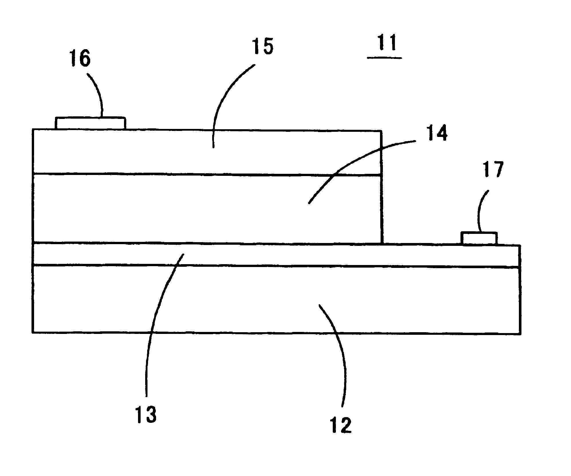
Thus, a p-type ZnO film doped with the Group I element Cu and the Group VII element Mn was formed on th...


PUM

PropertyMeasurementUnit
thicknessaaaaaaaaaa
temperatureaaaaaaaaaa
luminescentaaaaaaaaaa

Abstract

A p-type ZnO film is formed on a sapphire substrate by RF magnetron sputtering in an atmosphere of a mixture of Ar and N2 gases, using a Zn metal target doped with Y2O3. The p-type ZnO film can be easily formed even on a large-sized substrate.

Description

1. Field of the InventionThe present invention relates to ZnO films, methods for manufacturing the ZnO films, and luminescent elements. In particular, the present invention relates to a p-type ZnO film, a method for manufacturing the ZnO film, and a luminescent element including the ZnO film.2. Description of the Related ArtDeposition of a ZnO film on a substrate has been studied for blue light-emitting diodes, solar cells, and the like. ZnO generally exhibits n-type conductivity as a result of adding a dopant such as Al. In order to form the pn junction, a p-type ZnO film is also necessary. However, it is difficult to form a p-type ZnO film.A method for forming a p-type ZnO film is disclosed in a literature entitled "p-Type Electrical Conduction in ZnO Thin Films by Ga and N Co doping" (Japan J. Appl. Phys., Vol. 38 (1999) pp. L1205-1207). In this method, a ZnO film is deposited on a glass substrate using a ZnO target doped with Ga while the inside of the vacuum chamber employed is...

Claims


Application Information

Patent Timeline
Patent Type & Authority Patents(United States)
IPC IPC(8): C30B23/02H01L21/363H01L21/02H01L33/00C30B29/16H01L21/203H01L21/205H01L33/28
CPCC30B23/02H01L33/0083C30B29/16H01L21/02554H01L21/0242H01L21/02579H01L21/02581H01L21/02631
Inventor KADOTA, MICHIOMIURA, TOSHINORI
Owner MURATA MFG CO LTD
Why Eureka
Try Eureka