

Thin film-structure and a method for producing the same
a film-structure and film-making technology, applied in the direction of microstructural devices, glass reforming devices, crystal growth processes, etc., can solve problems such as degradation of productivity, and achieve good productivity, reproducibility, and good shape-stability
- Summary
- Abstract
- Description
- Claims
- Application Information
AI Technical Summary
Benefits of technology
Problems solved by technology
Method used
Image

Examples
example 1
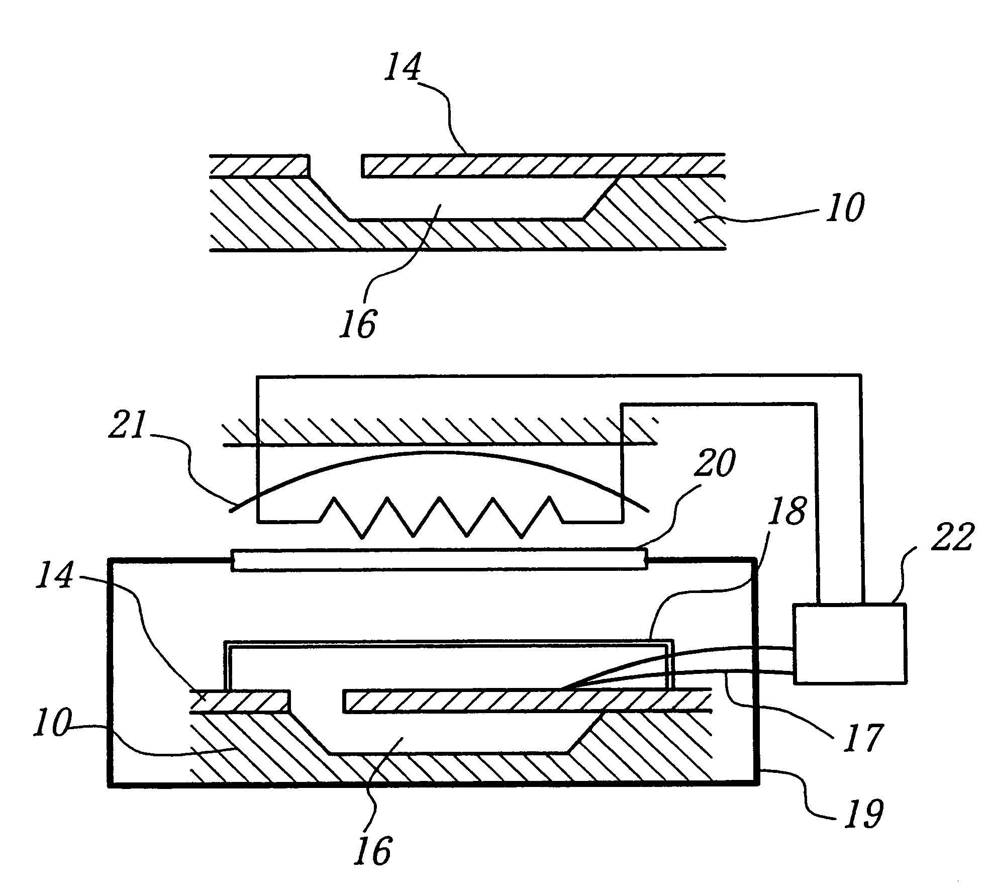
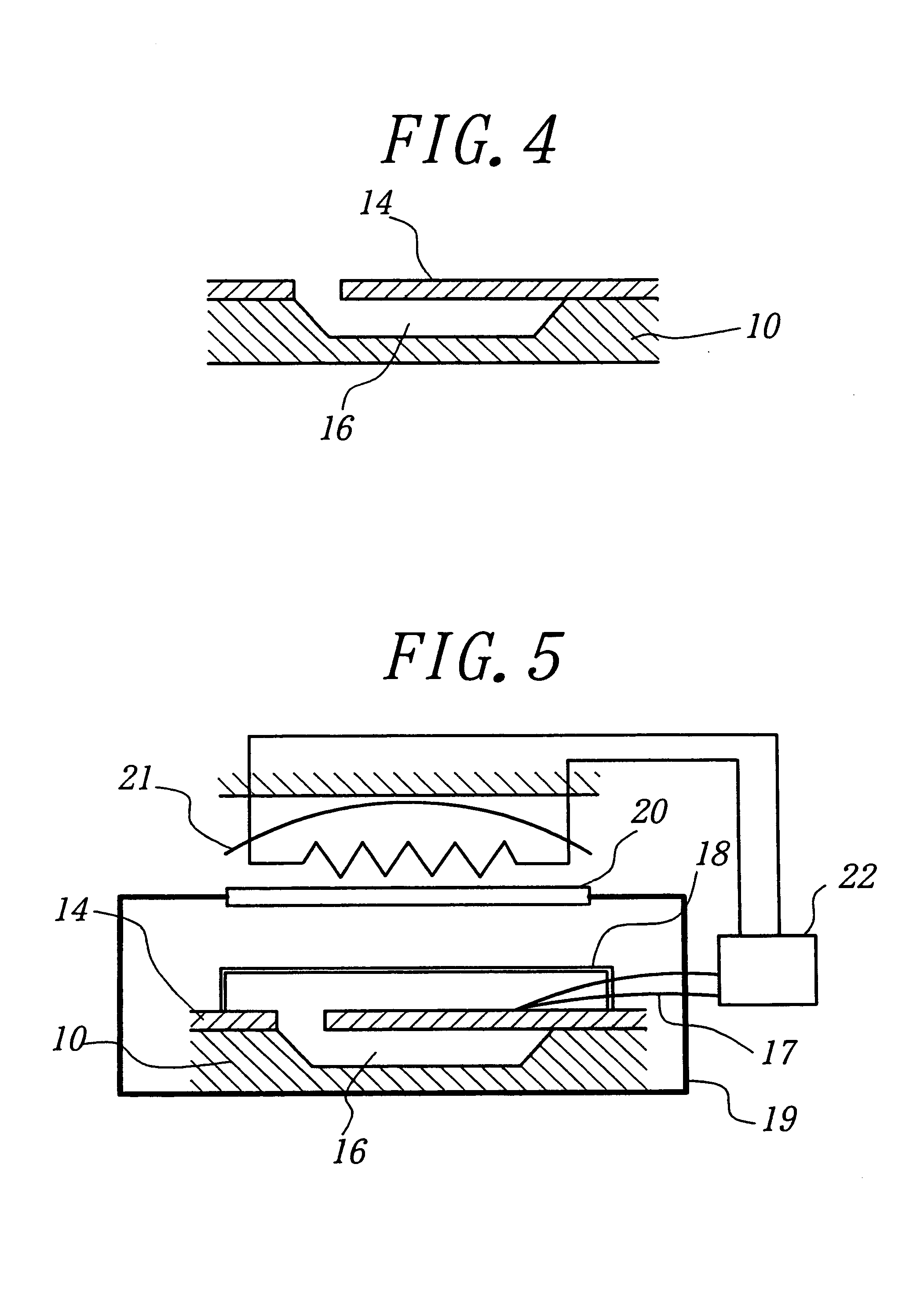
In this example, the thin film made of an amorphous material having an supercooled liquid phase region was deformed through its weight.
FIGS. 1-5 are process charts showing a producing process of the thin film-structure of this example.
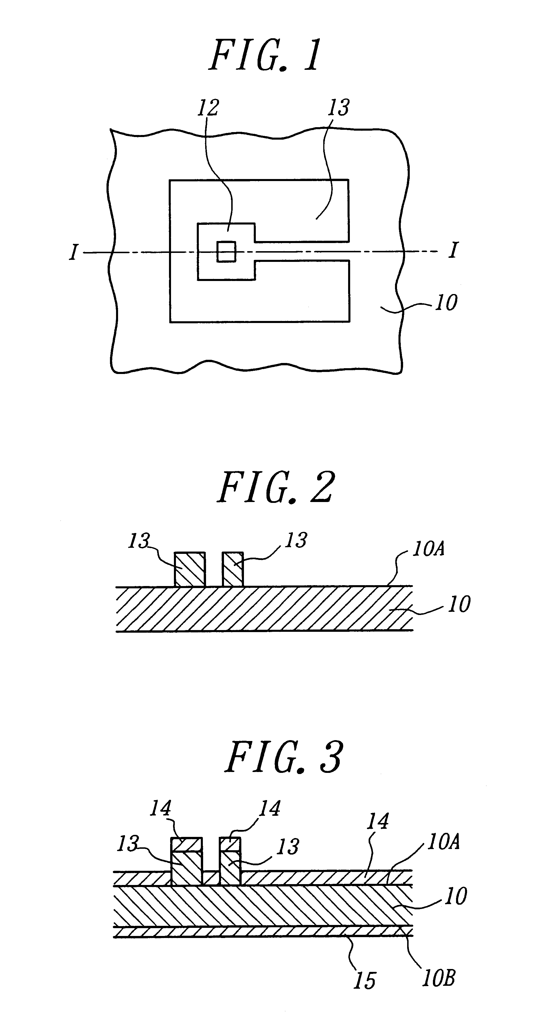
FIG. 1 is a plan view showing a first step in the producing method of the thin film-structure, and FIG. 2 is a cross sectional view taken on line I--I of FIG. 1. FIGS. 3-5 are cross sectional views showing steps after the step of FIGS. 1 and 2 with time.
A substrate 10 was composed of a single crystalline silicon wafer having a thickness of 200 .mu.m and a crystal orientation .
First of all, as shown in FIGS. 1 and 2, a polyimide film was formed in a thickness of 5 .mu.m, by a spin coat method, on a main surface 10A of the substrate 10, and an one side-fixed beam-like negative pattern 13 having a paddle 12 was formed by reactive ion etching (RIE). Then, as shown in FIG. 3, a thin film 14 made of a Zr.sub.66 Cu.sub.33 Al metallic glass was formed in a thi...
example 2
In this example, the thin film made of an amorphous material having an supercooled liquid phase region was deformed by mechanical external force.
FIGS. 11-15 are process chart showing a producing process of the thin film-structure of thin example. FIG. 11 is a plan view showing a first step of the producing method of the thin film-structure according to the present invention. FIGS. 12-15 are cross sectional views showing successive steps after the step of FIG. 11 with time. FIG. 13 is a cross sectional view taken on line II--II of FIG. 12.
A substrate 40 was composed of a single crystalline silicon wafer having a thickness of 200 .mu.m and a crystal orientation .
As shown in FIG. 11, a resist was spin-coated in a thickness of 1 .mu.m on a main surface 40A of the substrate 40 and patterned by an exposing equipment to form a rectangular provisional layer 41. Then, a thin film 42 made of boron oxide (B.sub.2 O.sub.3) was formed in a thickness of about 2 .mu.m, by a CVD method, on the main...
example 3
In this example, the thin film made of an amorphous material having an supercooled liquid phase region was deformed by electrostatic external force.
FIGS. 16-20 are process chart showing a producing process of the producing method of the thin film-structure of this example. FIG. 16 is a plan view showing a first step of the producing method of the thin film-structure according to the present invention. FIGS. 17-20 are cross sectional views showing successive steps after the step of FIG. 16 with time. FIG. 18 is a cross sectional view taken on line III--III of the plan view in FIG. 17.
A substrate 50 was composed of a single crystalline silicon wafer having a thickness of 250 .mu.m and a crystal orientation .
First of all, as shown in FIG. 16, a Cr-film 51 was formed in a thickness of 50 nm, by a sputtering method, on a main surface 50A of the substrate 50. Then, a boron oxide-film 52 was formed in a thickness of about 2 .mu.m, by a CVD method, on the Cr-film 51.
Next, as shown in FIGS. ...
PUM
| Property | Measurement | Unit |
|---|---|---|
| temperature | aaaaa | aaaaa |
| glass-transition temperature | aaaaa | aaaaa |
| tensile stress | aaaaa | aaaaa |
Abstract
Description
Claims
Application Information