Method of etching a trench in a silicon-on-insulator (SOI) structure

a technology of silicon-on-insulator and trench, which is applied in the direction of decorative surface effects, electrical appliances, decorative arts, etc., can solve the problems of notching, particularly affecting the etching effect,

Inactive Publication Date: 2004-07-06
APPLIED MATERIALS INC
View PDF19 Cites 44 Cited by
  • Summary
  • Abstract
  • Description
  • Claims
  • Application Information

AI Technical Summary

Problems solved by technology

Scalloping is particularly a problem when the etched trench is to be used as a mold in a subsequent process and when the silicon trench surface is to be used in an optical component.
Another problem which occurs when etching a trench in silicon in an SOI (silicon-on-insulator) structure is known as notching.
As etching progresses, and there is little or no silicon left at the base of the trench to be etched in a vertical direction, lateral etching into the silicon sidewall at the bottom of the trench continues, resulting in a severely undercut, notched profile at the base of the trench.
Notching is particularly a problem when etching closely spaced trenches.
Therefore, the depth of trenches which may be etched using the single-step embodiment is typically limited by the thickness of the photoresist layer which can be applied.

Method used


Image

  • Method of etching a trench in a silicon-on-insulator (SOI) structure
  • Method of etching a trench in a silicon-on-insulator (SOI) structure
  • Method of etching a trench in a silicon-on-insulator (SOI) structure

Examples


Embodiment Construction

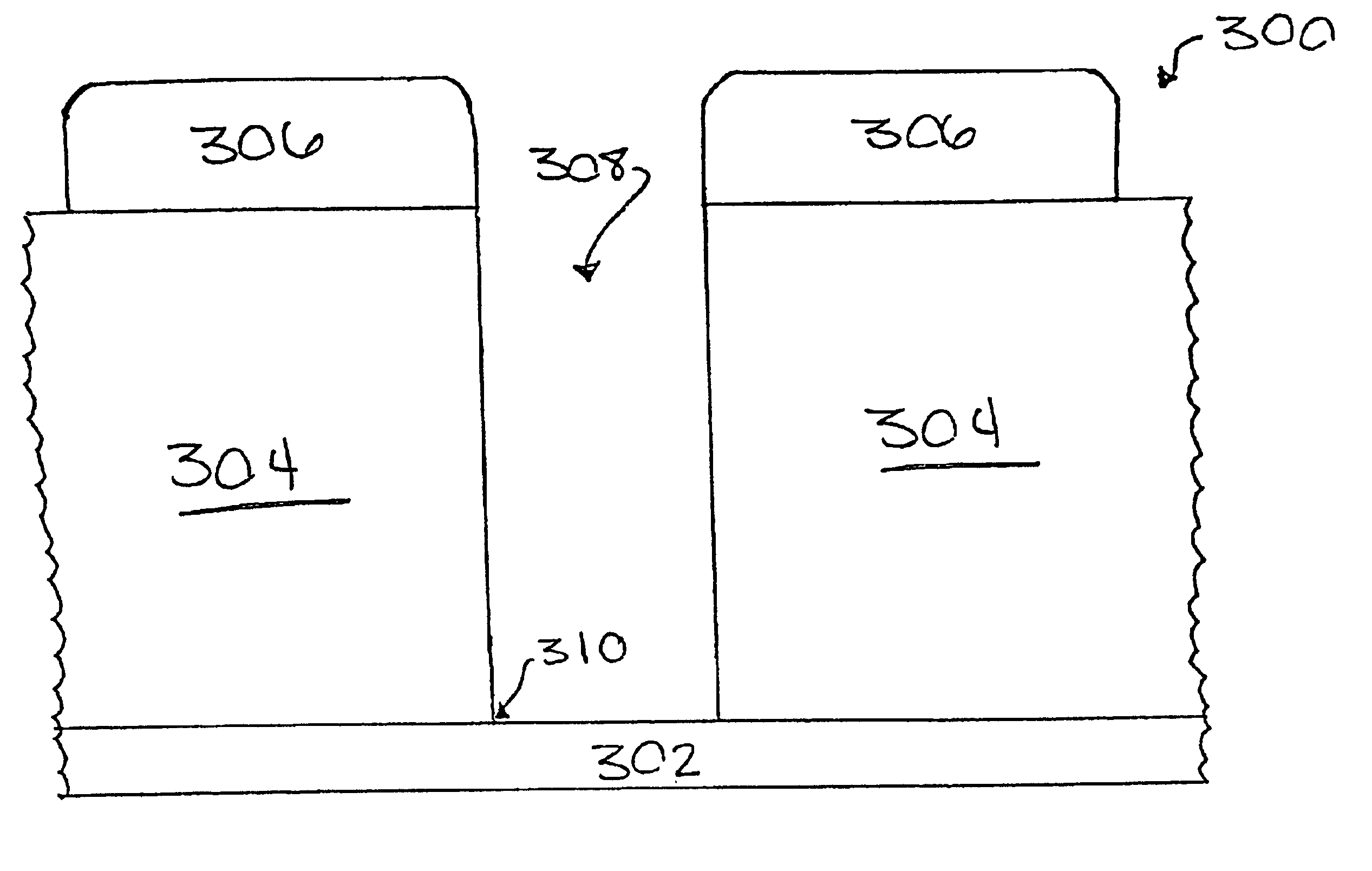
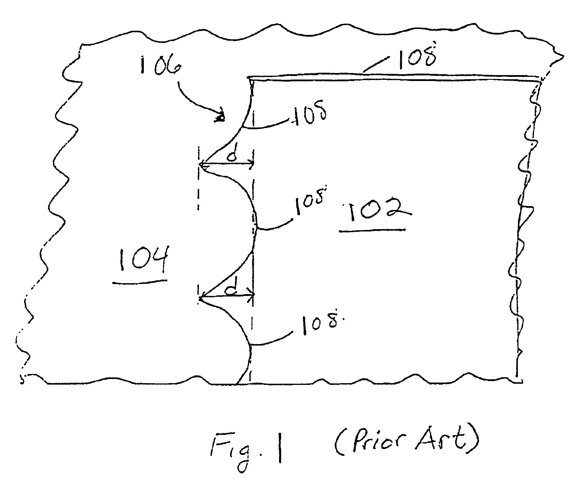
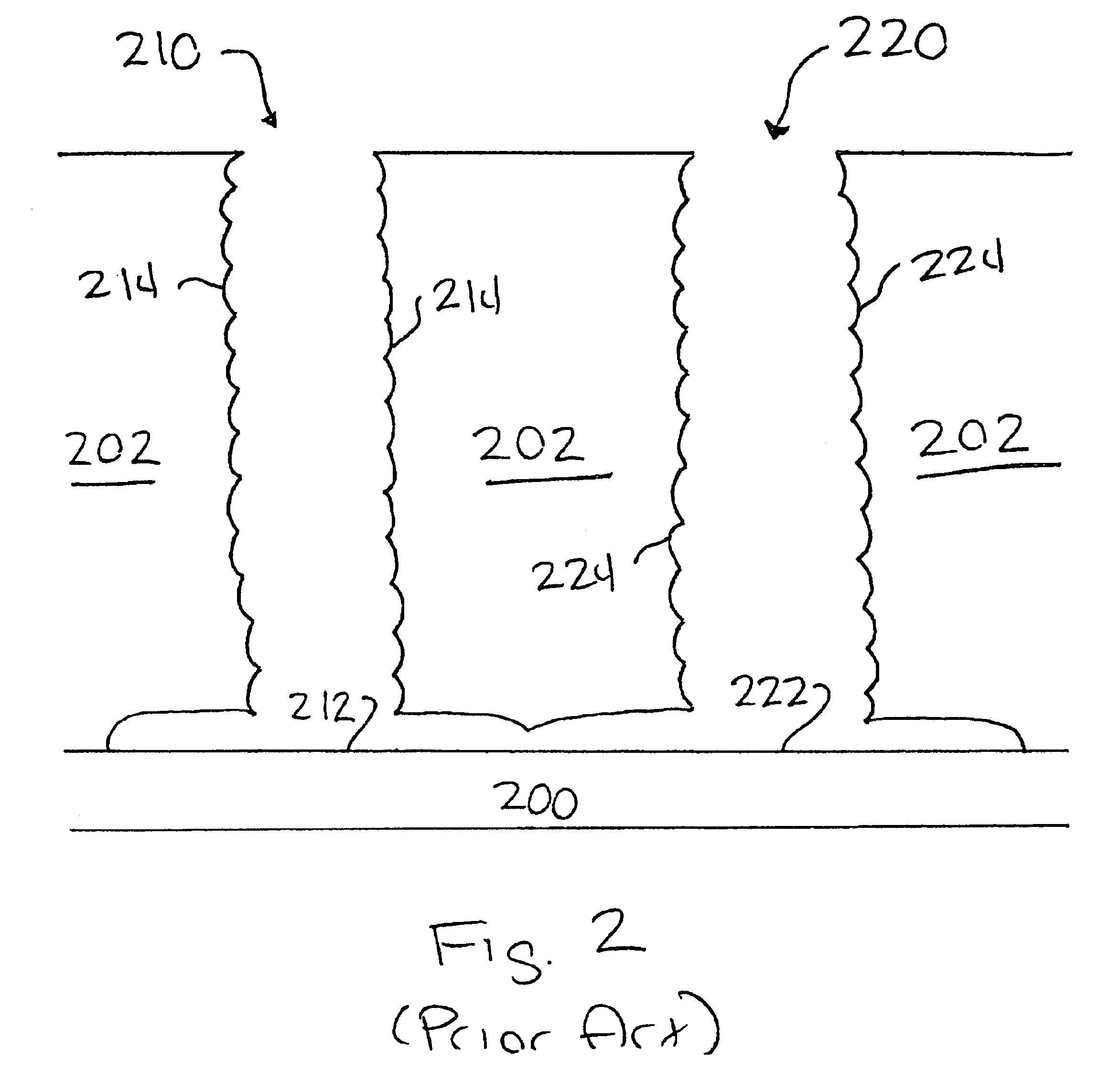
Disclosed herein is a method of eliminating notching at the silicon / dielectric interface of an SOI structure during etching of a trench in silicon. Exemplary processing conditions for performing the method of the invention are set forth below.

As a preface to the detailed description, it should be noted that, as used in this specification and the appended claims, the singular forms "a", "an", and "the" include plural referents, unless the context clearly dictates otherwise.

I. An Apparatus for Practicing the Invention

The embodiment example etch processes described herein were carried out in a CENTURA.RTM. Integrated Processing System available from Applied Materials, Inc., of Santa Clara, Calif. This apparatus is described in detail below; however, it is contemplated that other apparatus known in the industry may be used to carry out the invention.

FIG. 4A shows an elevation schematic of the CENTURA.RTM. Integrated Processing System. The CENTURA.RTM. Integrated Processing System is a f...


PUM

PropertyMeasurementUnit
feature sizeaaaaaaaaaa
pressureaaaaaaaaaa
volume %aaaaaaaaaa

Abstract

Disclosed herein is a method of etching a trench in silicon overlying a dielectric material which reduces or substantially eliminates notching at the base of the trench, while reducing scalloping on the sidewalls of the trench. The method comprises etching a first portion of a trench by exposing a silicon substrate, through a patterned masking layer, to a plasma generated from a fluorine-containing gas. This etching is followed by a polymer deposition step comprising exposing the substrate to a plasma generated from a gas which is capable of forming a polymer on etched silicon surfaces. The etching and polymer deposition steps are repeated for a number of cycles, depending on the desired depth of the first portion of the trench. The final portion of the trench is etched by exposing the silicon to a plasma generated from a combination of a fluorine-containing gas and a polymer-forming gas.

Description

1. Field of the InventionThe present invention pertains to a method of etching a trench in a silicon-on-insulator (SOI) structure. In particular, the present invention is a method of etching a trench in silicon overlying a dielectric material, where etching is performed using a plasma generated from a combination of a fluorine-containing etchant gas and a passivation gas.2. Brief Description of the Background ArtDeep trench silicon etching is one of the principal technologies currently being used to fabricate microstructure devices, and is an enabling technology for many microelectromechanical systems (MEMS) applications. Currently, the most commonly used single-crystal silicon deep trench etch process is based upon a cyclic plasma etch / polymer deposition method. The process enables the removal of at least one micron (1 .mu.m) of silicon per etch cycle. During the etch portion of the etch / deposition process, the principal etchant is often SF.sub.6, which may be used in combination w...

Claims


Application Information

Patent Timeline
Patent Type & Authority Patents(United States)
IPC IPC(8): C03C25/68H01L21/02H01L21/00H01L21/302H01L21/461H01L21/3065
CPCH01L21/30655
Inventor NALLAN, PADMAPANI C.KUMAR, AJAYKHAN, ANISUL H.YANG, CHAN-SYUN DAVID
Owner APPLIED MATERIALS INC
Why Eureka
Try Eureka