Data latch circuit having anti-fuse elements

a latch circuit and anti-fuse element technology, applied in the direction of computation using denominational number representation, pulse technique, instruments, etc., can solve the problem of difficult to judge whether the anti-fuse element is conductive or non-conductive, and it is difficult to perfectly exclude the defects of some memory cells during the manufacturing of the memory circui

Inactive Publication Date: 2004-07-06
NEC ELECTRONICS CORP
View PDF7 Cites 24 Cited by
  • Summary
  • Abstract
  • Description
  • Claims
  • Application Information

AI Technical Summary

Problems solved by technology

In an LSI including a memory circuit, it is difficult to perfectly exclude defects in some of the memory cells during manufacturing the memory circuit.
The anti-fuse elements are superior to the EPROM elements which require a large number of fabrication steps and thus the increased costs thereof.
However, there is a problem in the conventional anti-fuse elements that the anti-fuse elements have an average resistance around several hundreds of ohms after the dielectric breakdown, wherein some anti-fuse elements may have several tens of kilo-ohms at the maximum, although this is a relatively rare case.
In the case of several tens of kilo-ohms for the resistance of the anti-fuse elements, the judgement whether the anti-fuse elements are conductive or non-conductive is difficult and must be performed by using a detector having a higher sensitivity.

Method used


Image

  • Data latch circuit having anti-fuse elements
  • Data latch circuit having anti-fuse elements
  • Data latch circuit having anti-fuse elements

Examples


first embodiment

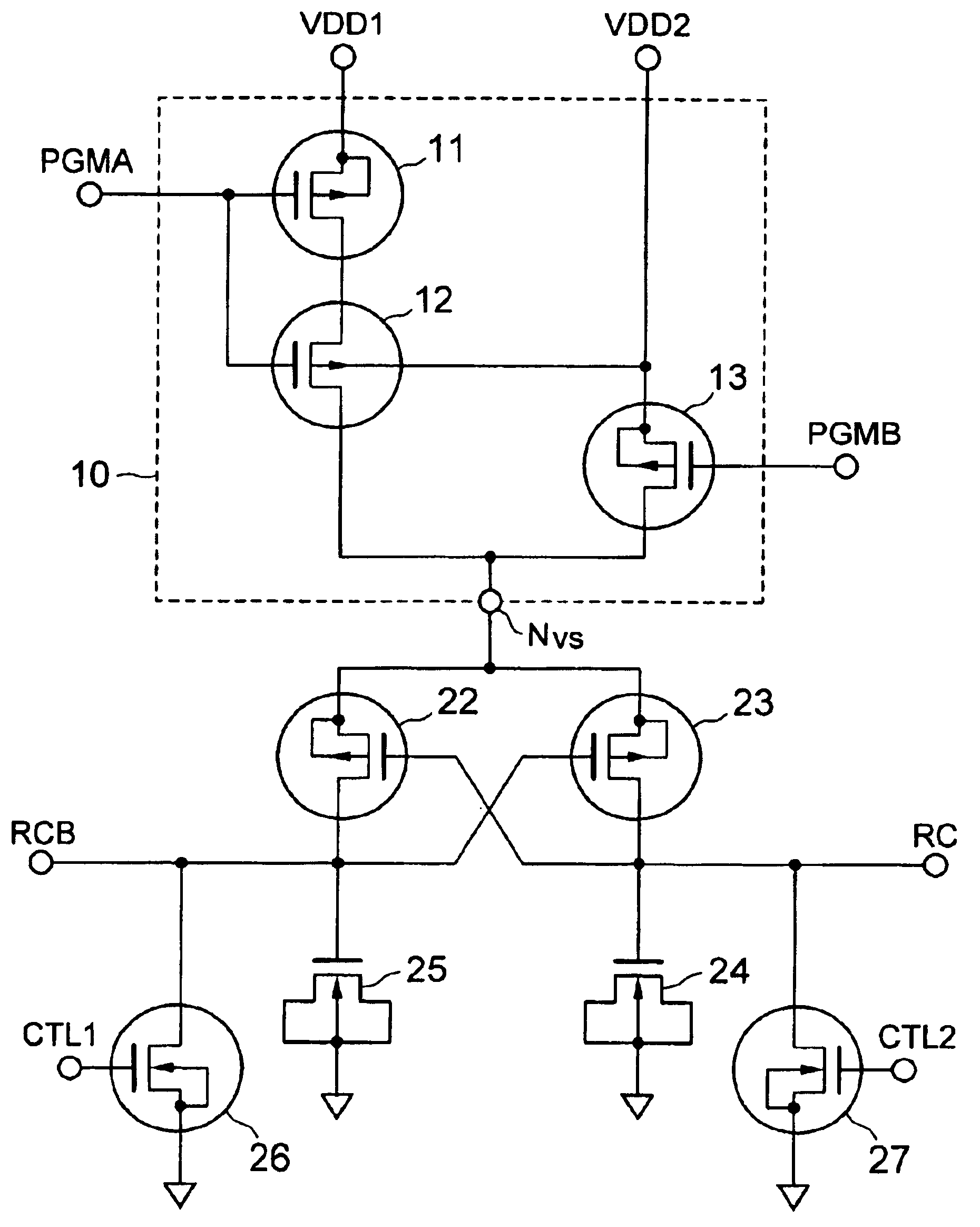
Referring to FIG. 1, a data latch circuit according to the present invention includes a voltage selection block 10, pMOSFETs 22 and 23 constituting a latching block, nMOSFETs 26 and 27 for setting programming data, and nMOSFETs 24 and 25 constituting capacitive anti-fuse elements to be programmed with a logic level "1" or "0". The logic level "1" to be stored in the data latch circuit effects dielectric breakdown of the gate insulation film of anti-fuse element 25, whereas logic level "0" effects dielectric breakdown of the gate insulation film of anti-fuse element 24.

The data latch circuit of FIG. 1 reads and latches the logic level stored in the anti-fuse elements 24 and 25 to deliver the latched logic level through output terminal RC and inverted latched logic level through output terminal RCB. The gate insulation films of nMOSFETs 24 and 25 have a first thickness, whereas the gate insulation films of pMOSFETs 22 and 23 and nMOSFETs 26 and 27 have a second thickness larger than t...

third embodiment

Referring to FIG. 5, a data latch circuit according to the present invention is similar to the data latch circuit of FIG. 1 except for the configuration of the voltage selection block.

More specifically, the voltage selection block 10a shown in FIG. 5 includes a pair of pMOSFETs 12 and 13. The pMOSFET 12 includes a gate insulation film having the second thickness, a source connected to the first power source VDD1, a gate receiving programming control signal PGMA, a drain connected to voltage selection node Nvs and a backgate connected to the second power source VDD2. The pMOSFET 13 includes a gate insulation film having the second thickness, source and backgate connected together to the second power source VDD2, a gate receiving programming control signal PGMB, and a drain connected to voltage selection node Nvs.

In the voltage selection block 10a, if the voltage of the second power source VDD2 becomes lower than the voltage of the first power source VDD1 due to an accidental cause su...

sixth embodiment

Referring to FIG. 8A, there is shown a semiconductor chip implementing a semiconductor integrated circuit including a remedy circuit 49 in a memory macro block 42, the remedy circuit 49 including a plurality of data latch circuits according to a

The semiconductor chip 41 mounts thereon the memory macro block 42, a plurality of internal logic macro blocks 43, I / O circuit blocks 44, power I / O pad 45 for the first power source VDD1, power I / O pad 46 for the second power source VDD2, and signal I / O pads 47. The I / O circuit block 44 receives both the voltages of the first and second power sources VDD1 and VDD2 from power I / O pads 45 and 46, respectively, whereas the logic macro block 43 receives the normal operating voltage Vop of the first power source VDD1 from the power I / O pad 45. The signals input through the signal I / O pads 47 are delivered to the logic macro blocks 43 after voltage conversion in the I / O circuit blocks 44 to the normal operating voltage Vop. The signals delivered fr...


PUM


Abstract

A data latch circuit includes anti-fuse elements for storing remedy information therein as to replacement of defective memory cells by redundant memory cells. For programming the anti-fuse elements to a logic level "1" in a programming mode, control signals CTL1 and CTL2 are set at a low level and a high level, respectively, and programming control signals PGMA and PGMB are set at a high level and a low level, respectively. A voltage selection node Nvs delivers a programming voltage Vpp, lowering an output terminal RCB to effect dielectric breakdown of anti-fuse element 25, which assumes a low resistance. In a normal operation mode, programming voltages PUMA and PGMB are set at a low level and a high level, respectively, and both control signals CTL1 and CTL2 are set at a low level Voltage output node Nvs delivers the normal operating voltage, raising output terminal RC to a high level to thereby deliver the stored logic level "1".

Description

(a) Field of the InventionThe present invention relates to a data latch circuit having anti-fuse elements and, more particularly, to a data latch circuit having functions of programming anti-fuse elements with desired data and delivering the nonvolatile data stored in the anti-fuse elements.(b) Description of the Related ArtIn an LSI including a memory circuit, it is difficult to perfectly exclude defects in some of the memory cells during manufacturing the memory circuit. To remedy a product memory device including therein one or more defective memory cells, redundant memory cells are generally used in the memory device to replace the detective memory cells by the redundant memory cells.The remedy information as to the remedy of the defective memory cells by the redundant memory cells is stored in nonvolatile memory elements, such as EPROM elements which are electrically programmable, fuse elements which are fused by a critical current to assume an electrically open state, and anti...

Claims


Application Information

Patent Timeline
Patent Type & Authority Patents(United States)
IPC IPC(8): G11C17/18G11C29/00G11C17/14G11C11/413G11C29/04H01L21/82H01L21/822H01L27/04H01L27/10
CPCG11C17/18G11C29/848
Inventor TAKAMI, SHINYA
Owner NEC ELECTRONICS CORP
Why Eureka
Try Eureka