Liquid crystal display panel

Inactive Publication Date: 2004-07-27
CITIZEN WATCH CO LTD
View PDF9 Cites 12 Cited by
  • Summary
  • Abstract
  • Description
  • Claims
  • Application Information

AI Technical Summary

Problems solved by technology

For this reason, in the case of a liquid crystal display panel using, for example, twisted nematic (TN) liquid crystal in a liquid crystal layer, it has been possible to effect consistent display across the entire area of a display region in a condition wherein no voltage is applied to the liquid crystal layer, but impossible to do so in a condition wherein a voltage is applied thereto because the voltage cannot be applied to regions of the gaps where no electrode has been installed.
However, if, for effecting display at any of the pattern display portions, a voltage is intended to be applied to a signal electrode and an opposite electrode for the relevant pattern display portion, this will cause a problem that, because the voltage is applied via a wiring at connected to the signal electrode, the voltage will be applied to a portion of the liquid crystal layer between the wiring electrode and the opposite electrode as well, so that a region of the wiring electrode as well as the relevant pattern display portion is turned into a display state.
However, if the same are rendered too thin, this will increase electrical resistance, causing a problem of poor responsivity in display.
Consequently, it follows that the entire region of the liquid crystal layer, other than the regions of the necessary display portions, cannot be rendered transparent.
In particular, in the case of using the scattering type liquid crystal layer for the liquid crystal layer, the structure of the transparent solids is broken down when subjected to rapid changes in temperature, and as a result, there arises a risk that regions where a transparent state does not occur even when a voltage is applied will occur to the periphery of the w

Method used


Image

  • Liquid crystal display panel
  • Liquid crystal display panel
  • Liquid crystal display panel

Examples


modification example 2

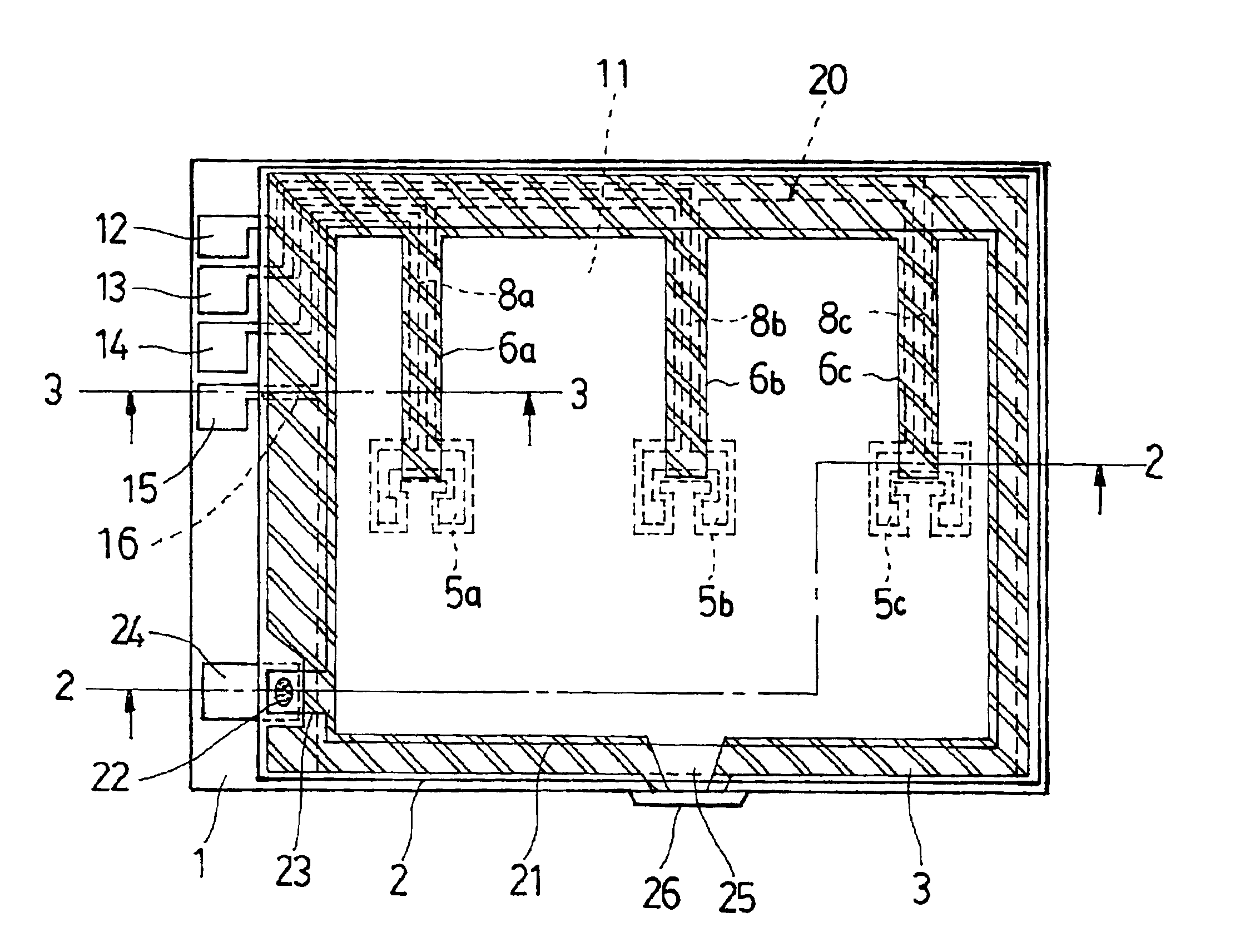
FIG. 11 shows another example of a liquid crystal display panel devised for preventing defects from occurring to the periphery of wiring sealing sections. In FIG. 11 as well, parts corresponding to those in FIGS. 1 to 9 are denoted by like reference numerals for convenience in description.

In this example, a peripheral sealing section 3 is formed of a sealing material different from that for wiring sealing sections 6a, 6b, 6c. That is, the wiring sealing sect 6a, 6b, 6c are formed of a sealing material lower in hardness, and softer (greater in elastic coefficient) than that for the peripheral sealing section 3.

As described hereinbefore, the peripheral sealing section 3 has functions of hermetically sealing a liquid crystal layer, keeping a given spacing between a first substrate and a second substrate, and protecting the liquid crystal layer from an ambient environment, and accordingly, an epoxy resin based adhesive with moderate hardness is used as the sealing material thereof.

For t...

second embodiment

Subsequently, a second embodiment of a liquid crystal display panel according to the invention, and a modification example thereof are, described with reference to FIGS. 13 to 15. In the figures as well, parts corresponding to those of the first embodiment, shown in FIGS. 1 to 11, are denoted by like reference numerals, and description thereof is omitted or simplified.

FIG. 13 is a plan view similar to FIG. 1 showing the second embodiment of the liquid crystal display panel according to the invention, and FIG. 14 is a sectional view taken along line 14--14 in FIG. 13, showing different cross sections thereof in the same plane.

The liquid crystal display panel according to the second embodiment is also a case wherein the present invention is applied to a liquid crystal display module used for a viewfinder of a camera, in which the liquid crystal display panel is provided with a light source causing light to fall on a liquid crystal layer from a side face of the liquid crystal display p...

modification example

A modification example wherein the liquid crystal display panel according to the second embodiment of the present invention is partially modified is described hereinafter with reference to FIG. 15. FIG. 15 is a sectional view of the modification example similar to FIG. 14.

This liquid crystal display panel differs from the liquid crystal display panel shown in FIGS. 13 and 14 only in that an ultraviolet cutoff film 41 is installed on the external face of the first substrate 1 and the second substrate 2, respectively.

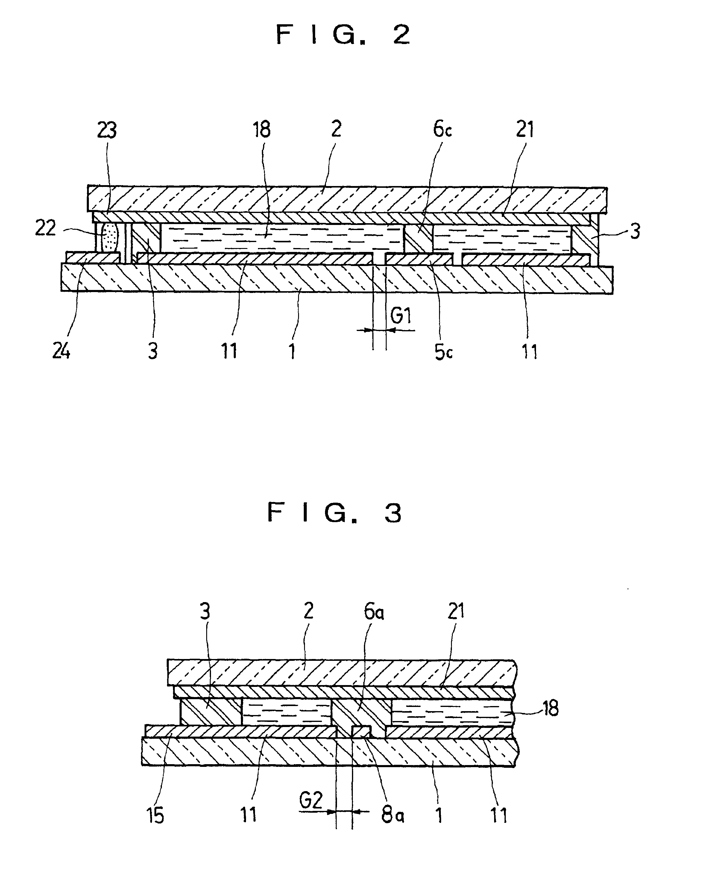
With these liquid crystal display panels, the smaller the width of a gap G3 formed between a target electrode 5b (the same applies to 5a and 5c) and a peripheral electrode 11 is, the easier a transparent state can be caused to occur over the entire display region. However, in order to enable a viewer to recognize beforehand a location of a target pattern for auto focus, it is preferable that the target pattern can be dimly seen, and accordingly, the width of the gap G3 ha...


PUM

PropertyMeasurementUnit
Coloraaaaaaaaaa
Shapeaaaaaaaaaa
Electric potential / voltageaaaaaaaaaa

Abstract

A liquid crystal display panel fabricated by bonding a first substrate and a second substrate together with a peripheral sealing section, providing a given spacing therebetween. A signal electrode is disposed so as to oppose an opposite electrode, and a liquid crystal layer is sealed in-between the spacing such that a transmittance thereof increases by applying a voltage thereto. The signal electrode is composed of target electrodes, wiring electrodes, and a peripheral electrode, and wiring sealing sections formed of a transparent sealing material are installed in regions where wiring electrodes are opposed to the opposite electrode such that a transmittance of the regions is always substantially equal to that of regions of the liquid crystal layer where a voltage is applied, thereby enabling a transmitting state to occur to the entire area of a display region in a condition wherein no voltage is applied.

Description

The present invention relates to a liquid crystal display panel forming a part of a liquid crystal display device, and more particularly, to a liquid crystal display panel suited for displaying patterns (characters, mark graphics, and so forth) in the shape as required in cloudy white or black, or in the form of a colored pattern against a transparent background.DESCRIPTION OF THE RELATED ARTAs liquid crystal display devices, using a liquid crystal display (LCD) panel, have advantages of low-profile shape, light weight, and further, very low power consumption, these devices have come to be used as display devices for a wide variety of equipment including various kinds of portable electronic equipment such as a tabletop calculator, cellular phone, wrist watch, camera, video camera, note-type personal computer, and so forth.With such a liquid crystal display panel, a pair of transparent substrates are bonded together by a sealing section provided on the periphery of a display region w...

Claims


Application Information

Patent Timeline
IPC IPC(8): G02F1/13G02F1/1343G02F1/1334
CPCG02F1/134309G02F1/1334
Inventor SEKIGUCHI, KANETAKA
Owner CITIZEN WATCH CO LTD
Why Eureka
Try Eureka