Puddle etching method of thin film by using spin-processor

a technology of etching method and spin-processor, which is applied in the direction of cleaning hollow objects, chemistry apparatus and processes, and using liquids to clean hollow objects, etc., can solve the problems of wasting a lot of etching solution, not being suitable for large-diameter wafers, and not being uniform enough

Inactive Publication Date: 2004-09-21
GRAND PLASTIC TECH
View PDF5 Cites 19 Cited by
  • Summary
  • Abstract
  • Description
  • Claims
  • Application Information

AI Technical Summary

Problems solved by technology

The batch method do not suitable to large diameter wafers, the single wafer spin etch is suitable to diameter above 8 inches.
However, supplying etching solution to the spinning wafer will waste a lot of etching solution, the uniformity is not good enough, the reason is that the staying time of the etching solution on the center and on the periphery of the wafer is different.
Using dry etching has high value of equipment and special gas problem, and dry etching is not suitable if isotropic or selective etching is required.

Method used


Image

  • Puddle etching method of thin film by using spin-processor
  • Puddle etching method of thin film by using spin-processor
  • Puddle etching method of thin film by using spin-processor

Examples


first embodiment

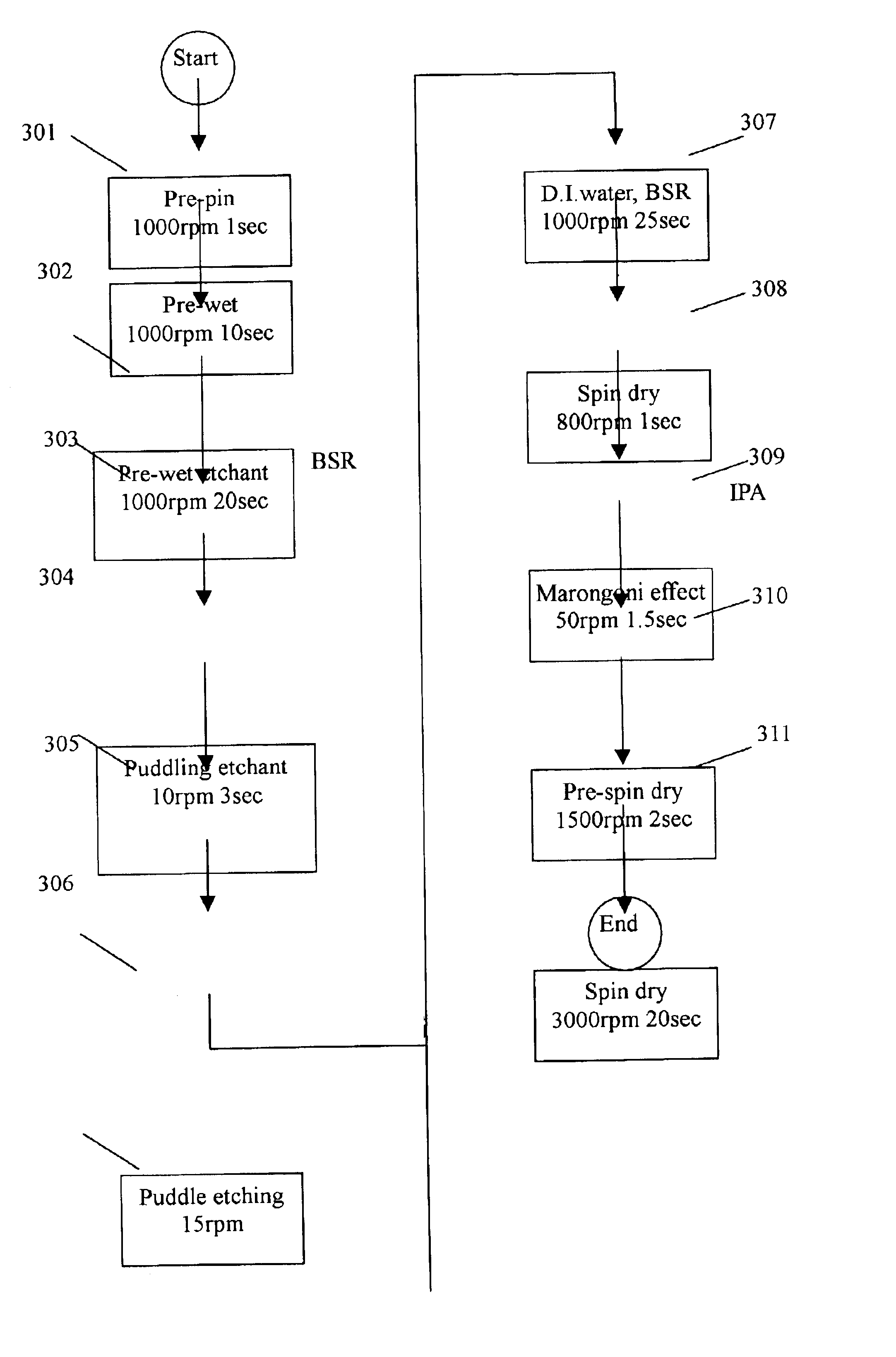
the present invention made use of etching silicon dioxide as an example. As the flow chart in FIG. 3, which explain the process of puddle etching. In step 301, load a wafer into a spin processor and spin with speed of 800-1200 rpm. In step 302, inject D.I, water and spin at a speed of 800-1200 rpm to pre-wet the wafer. In step 303, inject etching solution from the front side injection pipe 10 and back side rinse (BSR) with an injection rate of 600 cc / min and spin with 800-1200 rpm to remove the thin film on the surface and the photo-resist on the back-side of the wafer for 10-20 min., the speed may not be too low such that the photo-resist can carry out the particles on the wafer. In step 304, keep the wafer spin at a speed of 800-1200 rpm, stop supply etching solution to spin off the etching solution on the wafer for 1 sec. In step 305, the speed is slow down to 0-50 rpm, form puddle of etching solution by injected etching solution, the flow rate is 0.6-5 L / min for 3 sec., the quan...


PUM

PropertyMeasurementUnit
flow rateaaaaaaaaaa
diameteraaaaaaaaaa
flow rateaaaaaaaaaa

Abstract

The present invention discloses a puddle etching method of thin film. In a spin etching equipment, pre-wet the wafer by D.I. water and etch solution to remove the contamination and the upper layer of the film on the wafer. Then spin slowly (about 0-50 rpm) and inject etching solution to form a puddle of etching solution which will stay on the wafer, the wafer then keep spin slowly (about 0-50 rpm) such that the puddle of etching solution stay on the wafer and etching is going on by puddle etching. After the thin film is etched, the wafer is spin at higher speed, and D.I. water is injected to rinse. Then, IPA is used to remove the D.I. water by Marangoni effect. Finally raise the speed to dry the wafer.

Description

1. Field of the InventionThe present invention relates to a wet etching method of semiconductor processing, and more particularly, to a method for wet etching of thin film by forming a puddle of etching solution on the wafer in a spin processor2. Description of Relative Prior ArtIn semiconductor processing, batch wet etching or spin etch by using a single wafer spin processor is usually used to etch different kinds of thin film such as silicon dioxide, silicon nitride, silicon oxynitride, poly silicon, metal film, metal-silicide film, etc. The batch method do not suitable to large diameter wafers, the single wafer spin etch is suitable to diameter above 8 inches. However, supplying etching solution to the spinning wafer will waste a lot of etching solution, the uniformity is not good enough, the reason is that the staying time of the etching solution on the center and on the periphery of the wafer is different.Using dry etching has high value of equipment and special gas problem, an...

Claims


Application Information

Patent Timeline
Patent Type & Authority Patents(United States)
IPC IPC(8): C23F1/08H01L21/00H01L21/311
CPCC23F1/08H01L21/31111H01L21/6708H01L21/67115
Inventor TSUNG-KUEI, KANGHO, HSIEH YUEWANG, CHIH-CHENGSHIH-YI, HSIAO
Owner GRAND PLASTIC TECH
Why Eureka
Try Eureka