Dual-bit double-polysilicon source-side injection flash EEPROM cell

Inactive Publication Date: 2004-09-28
MA YUEH YALE +1
View PDF13 Cites 40 Cited by
  • Summary
  • Abstract
  • Description
  • Claims
  • Application Information

AI Technical Summary

Problems solved by technology

However, the definition of sharp process development associated with the and the delicate inter-polysilicon dielectric 153 of cell 150 is quite tedious.
However, because of its inherently high bit-line resistance, the virtual-ground array suffers from slower memory access speed.
A drawback of cell 200 is that it has a longer effective channel-length than the single-bit cell 100.
The lower read-current generally results in slower memory access time.
Despite the small size of the dual-bit cell 200, its costly triple-polysilicon manufacturing process and complicated six-terminal operations, make it an unattractive option for the cost sensitive high density applications.
However, because its operation requires high voltage in both positive and negative polarities, designing the array decoders to fit within the tight cell-pitch limits future advancement of this technology.
Also, because of its small read-current, the NAND-type array is more susceptible to noise immunity and suffers from slow sensing speed, and thus presents a greater challenge in achieving the target operation margins as technology scaling continues.

Method used


Image

  • Dual-bit double-polysilicon source-side injection flash EEPROM cell
  • Dual-bit double-polysilicon source-side injection flash EEPROM cell
  • Dual-bit double-polysilicon source-side injection flash EEPROM cell

Examples


Embodiment Construction

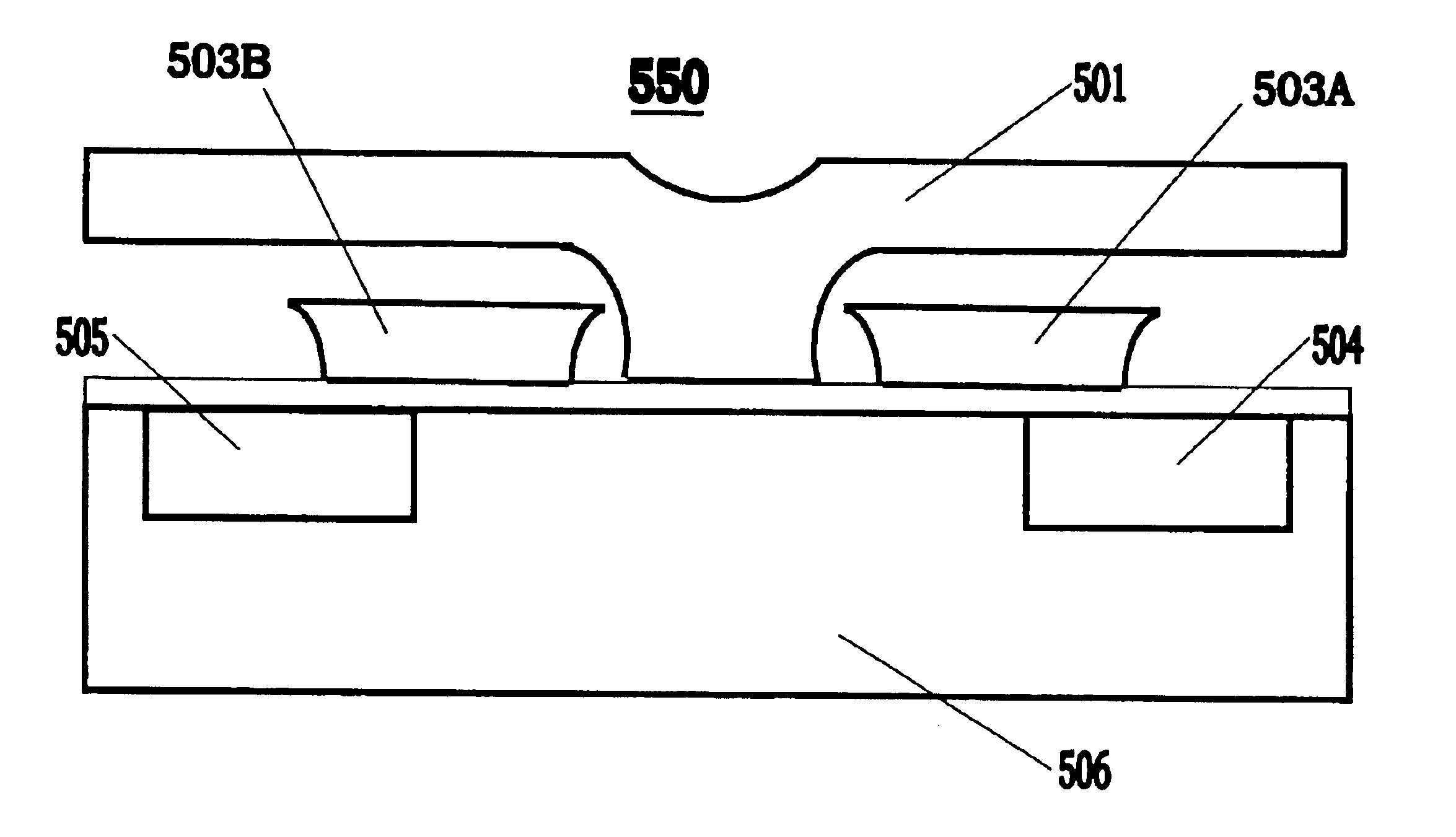
In accordance with the present invention, a double-polysilicon dual-bit cell structure includes two symmetrical floating gates for storing two bits of information. The two floating gates are horizontally separated by a portion of a select-gate. The two floating gates are insulated from the select-gate by an inter-gate dielectric. The inter-gate dielectric is generally thick (to achieve a relatively small capacitance between the floating gates and the select-gate), but has a "weak region" so that during erase-mode electrons can tunnel from the floating gate to the select-gate. The cell also includes a conduction channel beneath and insulated from the two floating gates and the intermediate select-gate portion. The channel is bounded by a pair of source / drain junctions formed in a cell body region. As described below, this is a four-terminal cell.

FIG. 3 shows a cross-section view of a dual-bit flash EEPROM cell structure 300 in accordance with one embodiment of the present invention. ...


PUM


Abstract

A four-terminal dual-bit double-polysilicon source-side injection flash EEPROM cell, capable of storing two bits of information includes a right junction (which can serve as a cell drain or a source), a left junction (which can serve as a cell source or drain), a select-gate, and two floating gates. The two floating gates are insulated from the select-gate by an inter-gate dielectric. The inter-gate dielectric has a "weak region" so that during erase-mode electrons can tunnel from the floating gate to the select-gate. The two bits in the cell are to be separately read or programmed, but are to be erased simultaneously. Programming of each bit is achieved through hot-carrier injection, while simultaneous erase of the two bits is achieved through electron-tunneling.

Description

This invention relates to semiconductor non-volatile memory devices, and more particularly to a dual-bit source-side injection cell which has two floating gates for storing two bits of information.,DESCRIPTION OF THE RELATED ARTThere are two types of hot-electron injection flash EEPROM cells, classified by the location of the charge injection in the programming mode. They are commonly referred to as "drain-side" and "source-side" injection cells. In a drain-side injection cell, electrons are injected onto the floating gate from a region in the source-drain channel near the drain junction; while in a source-side injection cell, electrons are injected onto the floating gate from a region in the source-drain channel near the source junction.Source-side injection cell has superior programming characteristics because it requires substantially lower programming current than the drain-side injection cell. Therefore, source-side injection cells are more suitable for low power and low voltag...

Claims


Application Information

Patent Timeline
IPC IPC(8): G11C16/04H01L29/66H01L29/788
CPCG11C16/0458H01L29/7887
Inventor MA, YUEH YALEPANG, CHAN-SUI
Owner MA YUEH YALE
Why Eureka
Try Eureka