
Method for joining conductive structures and an electrical conductive article

a technology of conductive structures and electrical conductive articles, applied in the field of joining semiconductor substrates, can solve the problems of low yield of fine-pitch small bumps, limited solder bump size, and high cost of substrate buildup

Inactive Publication Date: 2004-10-05
FUJITSU LTD
View PDF22 Cites 107 Cited by
  • Summary
  • Abstract
  • Description
  • Claims
  • Application Information

AI Technical Summary

Benefits of technology

The present invention provides an interconnect structure and method for joining semiconductor substrates using transient liquid alloy bonding. This interconnect structure and method offer a more reliable and efficient way to join semiconductor substrates compared to previous methods, such as soldering and brazing. The use of a transient liquid alloy bonding technique allows for the formation of a strong and durable bond between the substrates, even at high temperatures. The invention also includes a method for de-concentrating mechanical stain present at one or both of the top and bottom ends of each post to improve the bonding quality. Overall, the invention provides a more reliable and efficient way to join semiconductor substrates, which is important for the development of high-performance circuit boards and other electronic devices.

Problems solved by technology

Substrate buildup is expensive.
For typical solder printing methods, there is a limitation on the size of solder bumps, and the yield will be low for fine-pitch small bumps.
Furthermore, joints will be less reliable on micro-bumps.

Method used


Image

  • Method for joining conductive structures and an electrical conductive article
  • Method for joining conductive structures and an electrical conductive article
  • Method for joining conductive structures and an electrical conductive article

Examples


case ii

In Case II of FIGS. 53A-53B, the MCMs 204 are connected to two (2) daughter boards 206--206. The signal connections are through TF3DC 210 (see FIG. 57). The power / ground connections are directly through the MCM 204 substrates itself (see FIGS. 58-63). The daughter boards 206--206 are connected to the mother board 200 using the same arrangement as in Case I. The daughter boards 206--206 may arrange for the signal connections among the MCMs 204. With the daughter board 206, the structure of the mother board 200 can be simpler and the cost, cheaper.

case iii

In Case III of FIGS. 54A-54B, only one horizontal daughter board 206 is employed. The daughter board 206 may be connected to the mother board 200 through an area array connection 207 (for example, solder joints). The area array connection 207 is more preferable than Case II arrangement as the connection technology is simpler. The signal connections among the MCMs 204 may only go through one side of the MCM 204. The signal trace density in the daughter board 206 is higher than that in the Case II structure.

In Case IV of FIGS. 55A-55B, which is a combination of Case II and Case III, three (3) daughter boards 206--206--206 are employed. The structure of each of the daughter board 206 will be simpler. Also, the number of signal interconnect among the MCMs 204 can be higher if required.

Referring now to FIGS. 56-57 and as previously indicated, there is seen the connections between the MCMs 204 and the daughter board 206 (or the mother board 200). The signal connections are through the TF3...


PUM

PropertyMeasurementUnit
surface areaaaaaaaaaaa
melting pointaaaaaaaaaa

Abstract

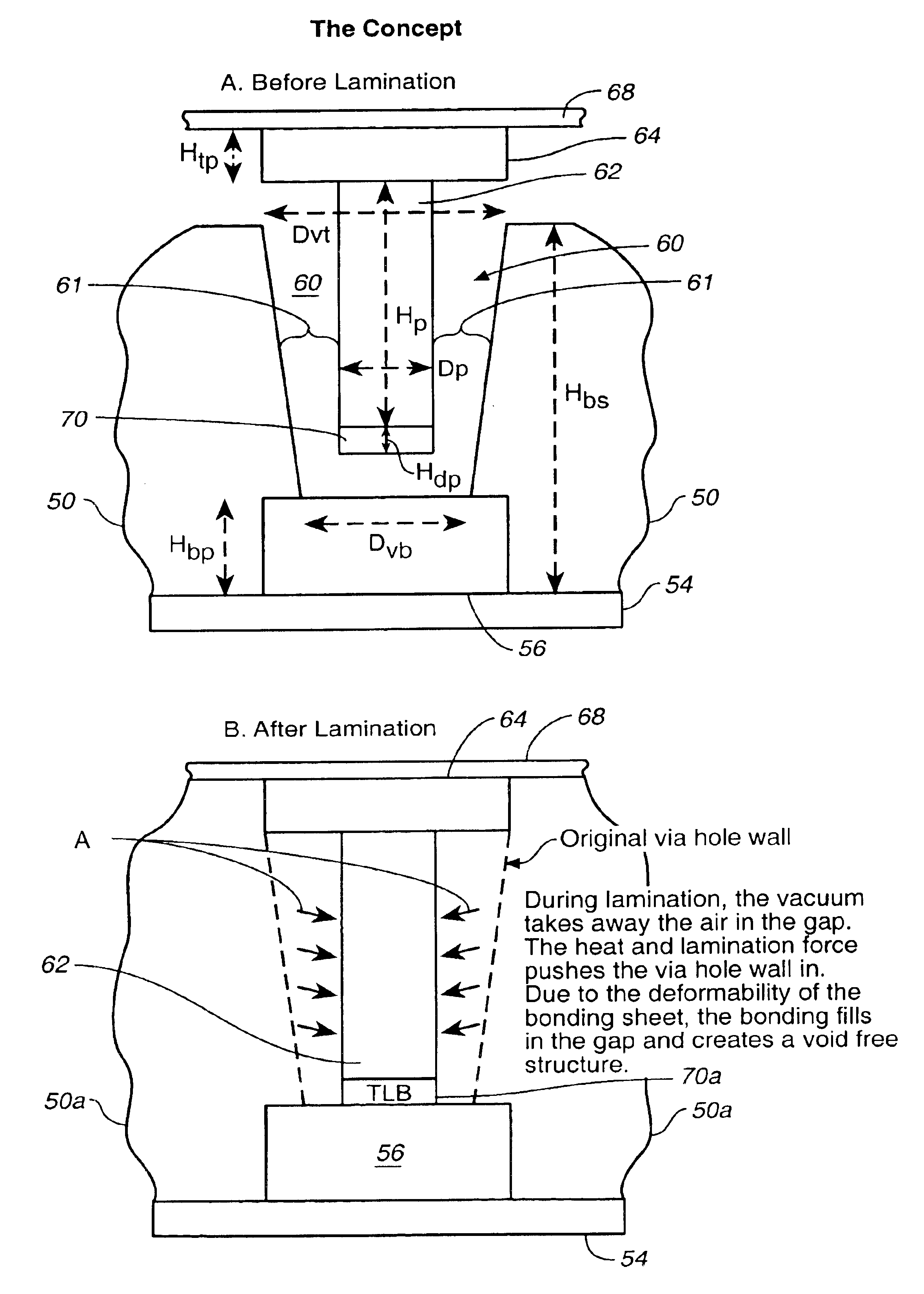
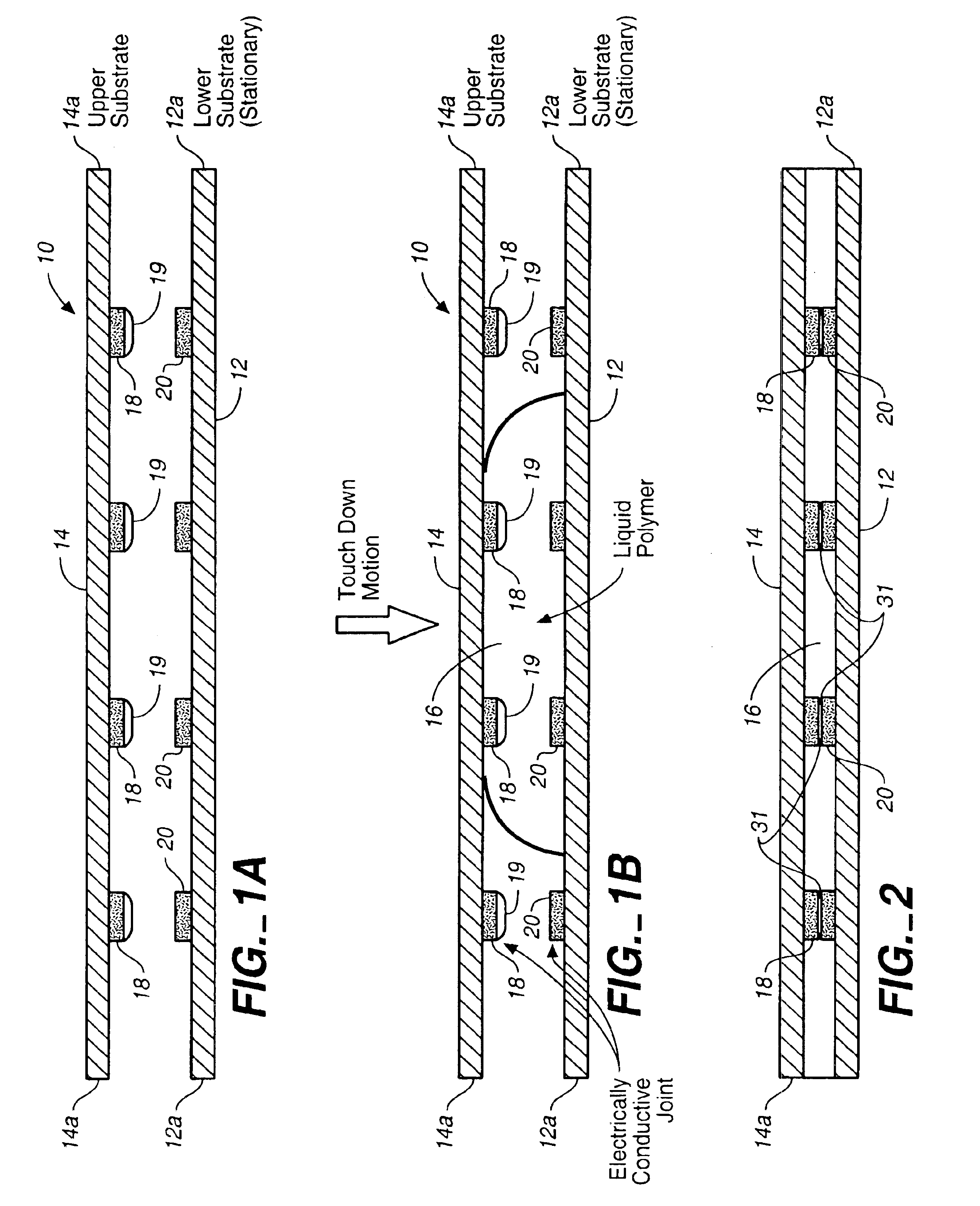
Embodiments of the invention include a method comprising disposing a thin metallic layer having a low melting temperature between one end of a conductive post on a substrate and a conducting structure on an opposing substrate. Heated platens in contact with the substrates can apply pressure and heat to the thin metallic layer and cause it to be entirely consumed and subsequently transformed into a bonding layer having a melting temperature higher than the melting temperature of the original thin metallic layer. Prior to, during, or after the conductive post is bonded to the conducting structure, the region around the conductive post and between the substrates may be filled with a dielectric material, such as polyimide.

Description

1. Field of the InventionThis invention is related to joining of semiconductor substrates. More specifically, the present invention provides an interconnect structure and method for joining or coupling together substrates employing transient liquid alloy bonding.2. Description of the Prior ArtA patentability investigation was conducted and the following U.S. Patents were discovered: U.S. Pat. No. 5,334,804 to Love et al.; U.S. Pat. No. 5,374,344 to Gall et al.; U.S. Pat. No. 5,374,469 to Hino et al.; U.S. Pat. No. 5,384,690 to Davis et al.; U.S. Pat. No. 5,421,507 to David et al.; U.S. Pat. No. 5,432,998 to Galasco et al.; U.S. Pat. No. 5,509,196 to Davis et al.; U.S. Pat. No. 5,620,782 to Davis et al.; U.S. Pat. No. 5,736,679 to Kresge et al.; U.S. Pat. No. 5,376,403 to Capote et al.; U.S. Pat. No. 5,128,746 to Pennisi et al.; U.S. Pat. No. 5,232,532 to Hori; U.S. Pat. No. 5,157,828 to Coques et al.; U.S. Pat. No. 5,187,123 to Yoshida et al.; U.S. Pat. No. 5,839,188 to Pommer; and ...

Claims


Application Information

Patent Timeline
Patent Type & Authority Patents(United States)
IPC IPC(8): B32B7/12H01L21/02H01L21/68H01L21/67H01L21/58H05K3/46H05K3/34H01L21/60
CPCB32B7/12H01L21/6835H01L24/83H05K3/4614H01L24/29H01L2221/68345H01L2221/68359H01L2224/16H01L2224/73253H01L2224/8319H01L2224/83855H01L2924/01002H01L2924/01004H01L2924/01005H01L2924/01013H01L2924/01015H01L2924/01027H01L2924/01029H01L2924/01039H01L2924/0104H01L2924/01047H01L2924/01049H01L2924/0105H01L2924/01051H01L2924/01073H01L2924/01078H01L2924/01079H01L2924/01082H01L2924/01322H01L2924/01327H01L2924/07802H01L2924/14H01L2924/19041H01L2924/19043H01L2924/30105H01L2924/3011H05K3/3489H05K2203/0759H01L2924/0132H01L2224/2919H01L2924/01006H01L2924/01023H01L2924/01024H01L2924/01033H01L2924/01072H01L2924/014H01L2924/0665H01L2224/29109H01L2224/29111H01L2224/81825H01L2224/83825Y10T29/49126H01L2924/00H01L2924/01031H01L2924/01083H01L2224/05568H01L2224/05573H01L2924/12042B32B15/08B32B37/1207B32B2457/14
Inventor LIU, KUO-CHUANLEE, MICHAEL G.
Owner FUJITSU LTD
Learn More