Integrated waveguide gratings by ion implantation

a technology of integrated waveguide gratings and ion implantation, which is applied in the direction of optical waveguide light guides, optical elements, coupling systems, etc., can solve the problems of inability to use routing systems or opto-electronic devices, and inability to achieve uniform photonic band gap crystal structures

Inactive Publication Date: 2004-11-09
INTEL CORP
View PDF42 Cites 12 Cited by
  • Summary
  • Abstract
  • Description
  • Claims
  • Application Information

AI Technical Summary

Problems solved by technology

However, because Fiber Bragg Gratings are created within the fiber itself, the applications are limited and therefore cannot be used in coupling systems, routing systems or opto-electronic devices.
Unfortunately, apodization is not currently possible with uniform photonic band gap crystal structures.
More importantly, because integrated waveguides and photonic crystals are often fabricated in semiconductors that absorb ultraviolet light, bleaching is not a practical means for generating index of refraction changes.

Method used


Image

  • Integrated waveguide gratings by ion implantation
  • Integrated waveguide gratings by ion implantation
  • Integrated waveguide gratings by ion implantation

Examples


Embodiment Construction

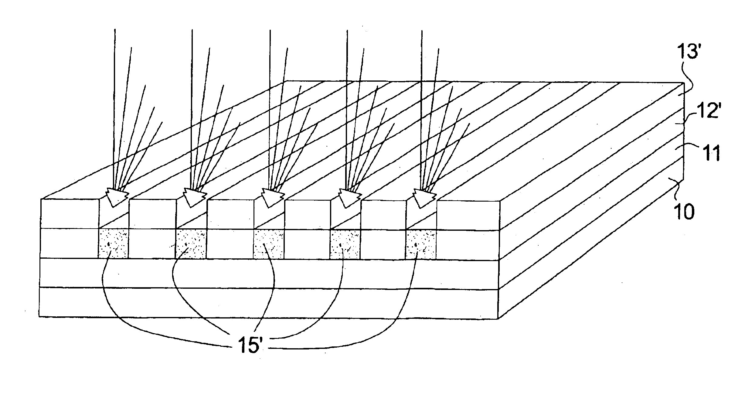
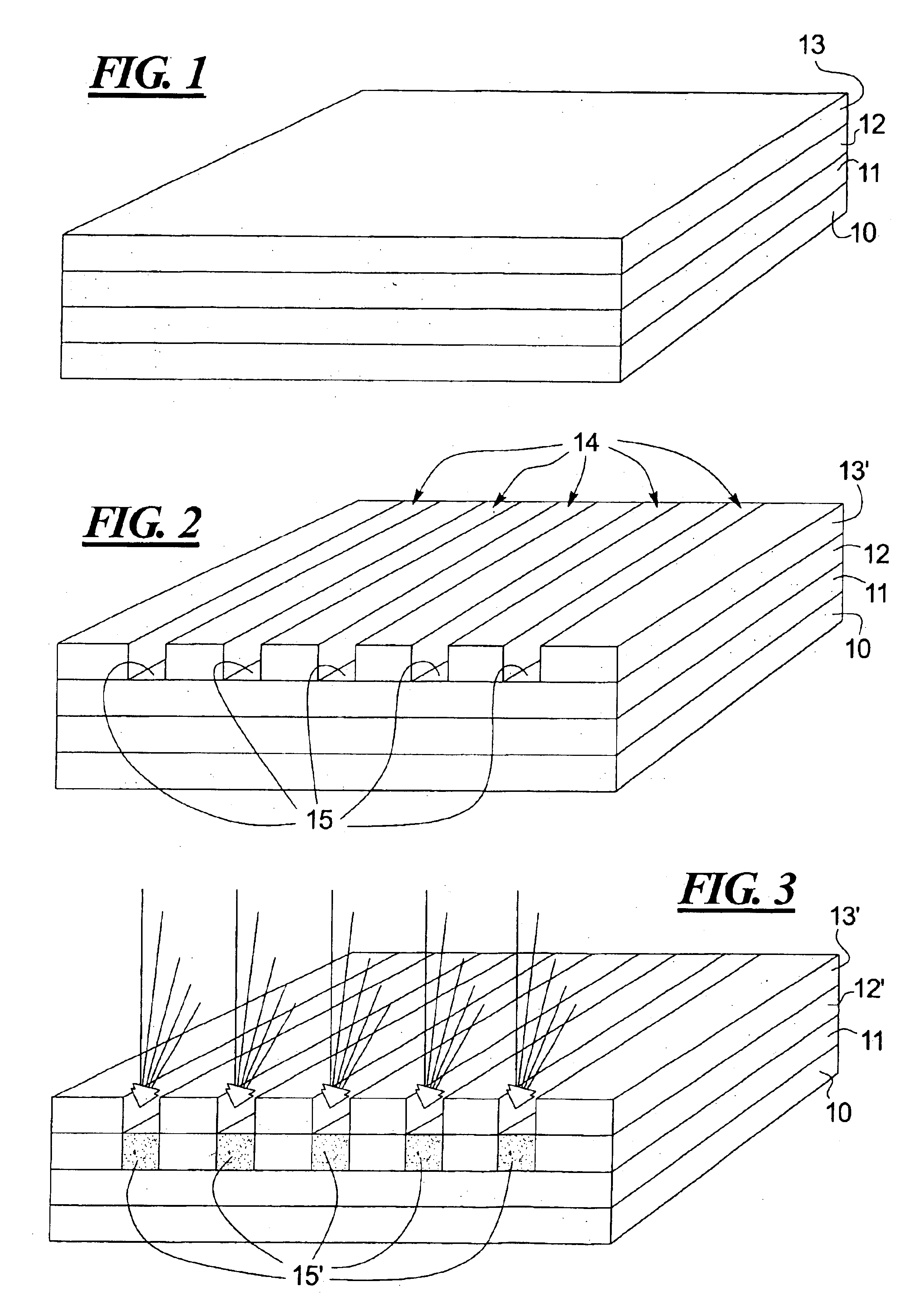
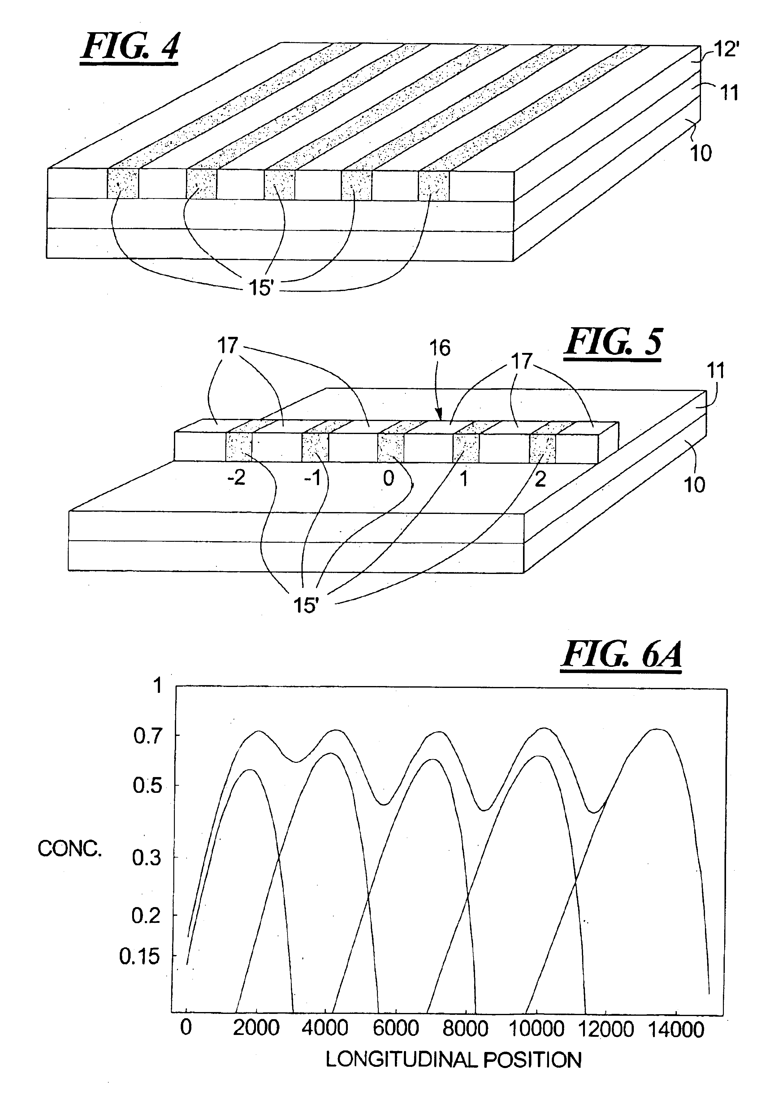
FIGS. 1-5 illustrate a novel method for fabricating an integrated semiconductor waveguide grating. Referring to FIG. 1, a lower cladding 11 is deposited on a substrate 10. A guide layer 12 is deposited on the lower cladding 11 and a mask layer 13 is deposited on the guide layer 12. Turning to FIG. 2, the mask layer 13 is patterned and etched to create a series of periodic structures, or transverse grooves shown generally at 14. The patterning is preferably carried out using a lithographic process although other patterning processes such as ablation, ruling, or other techniques will be apparent to those skilled in the art. The etching can be carried out using either a dry or a wet process, and varieties of both wet and dry etching will be apparent to those skilled in the art and will be dependent upon the material used for the guide and masking layers. Also as shown in FIG. 2, discrete transverse sections 15 of the guide layer 12 are exposed by the patterned mask layer 13.

Turning to ...


PUM

PropertyMeasurementUnit
lengthaaaaaaaaaa
lengthsaaaaaaaaaa
concentrationaaaaaaaaaa

Abstract

Integrated semiconductor waveguide gratings, methods of manufacture thereof and methods of apodizing thereof are described. A semiconductor waveguide grating includes a substrate, a cladding layer disposed on the substrate, a guide structure that includes a plurality of discrete transverse sections implanted with ions disposed between adjacent transverse sections substantially free of implanted ions.

Description

1. Technical FieldIntegrated semiconductor waveguide gratings are disclosed that are fabricated using ion implantation. Methods of fabricating integrated semiconductor waveguide gratings are disclosed that use ion implantation to form a refractive index grating along the length of the integrated semiconductor waveguide. Further, methods of apodizing integrated waveguide gratings are also disclosed.2. Description of the Related ArtThere is a wide-ranging demand for increased communications capabilities, including more channels and greater bandwidth per channel. The needs range from long distance applications such as telecommunications between two cities to extremely short range applications such as the data-communications between two functional blocks (fubs) in a semiconductor circuit with spacing of a hundred microns. Optical media, such as optical fibers or waveguides, provide an economical and higher bandwidth alternative to electrical conductors for communications. A typical opti...

Claims


Application Information

Patent Timeline
Patent Type & Authority Patents(United States)
IPC IPC(8): G02B6/124G02B6/13G02B6/132G02B6/134G02B6/136G02B6/12
CPCG02B6/124G02B6/132G02B6/136G02B6/1347G02B2006/12169
Inventor GOLDSTEIN, MICHAEL
Owner INTEL CORP
Why Eureka
Try Eureka