Method and system for all-optical signal regeneration
a technology of all-optical signal and regeneration method, which is applied in the field of all-optical signal regeneration method and system, can solve the problems of reduced signal-to-noise ratio (s/n), noise induced by amplified spontaneous emission (ase) occurring in the amplifier, and limited maximum transmission distan
- Summary
- Abstract
- Description
- Claims
- Application Information
AI Technical Summary
Benefits of technology
Problems solved by technology
Method used
Image
Examples
first embodiment
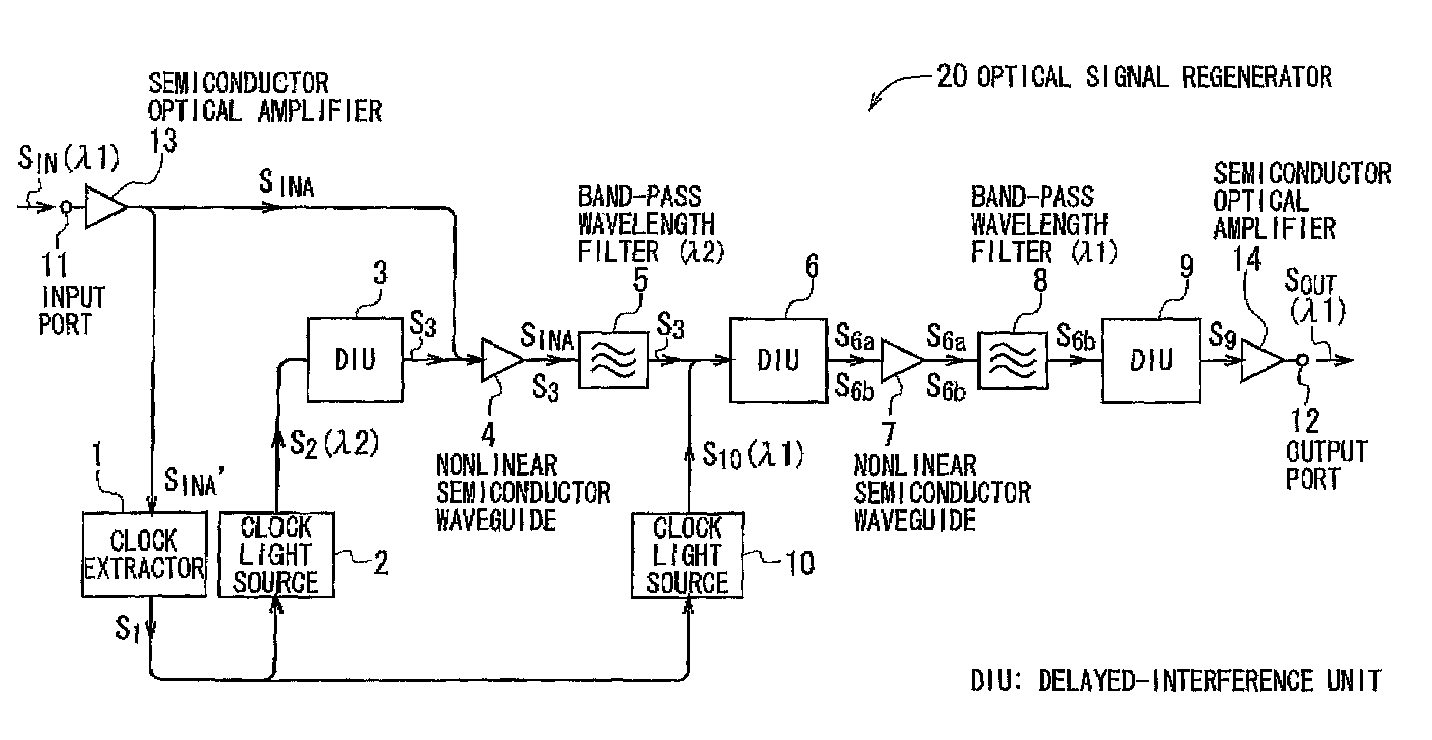
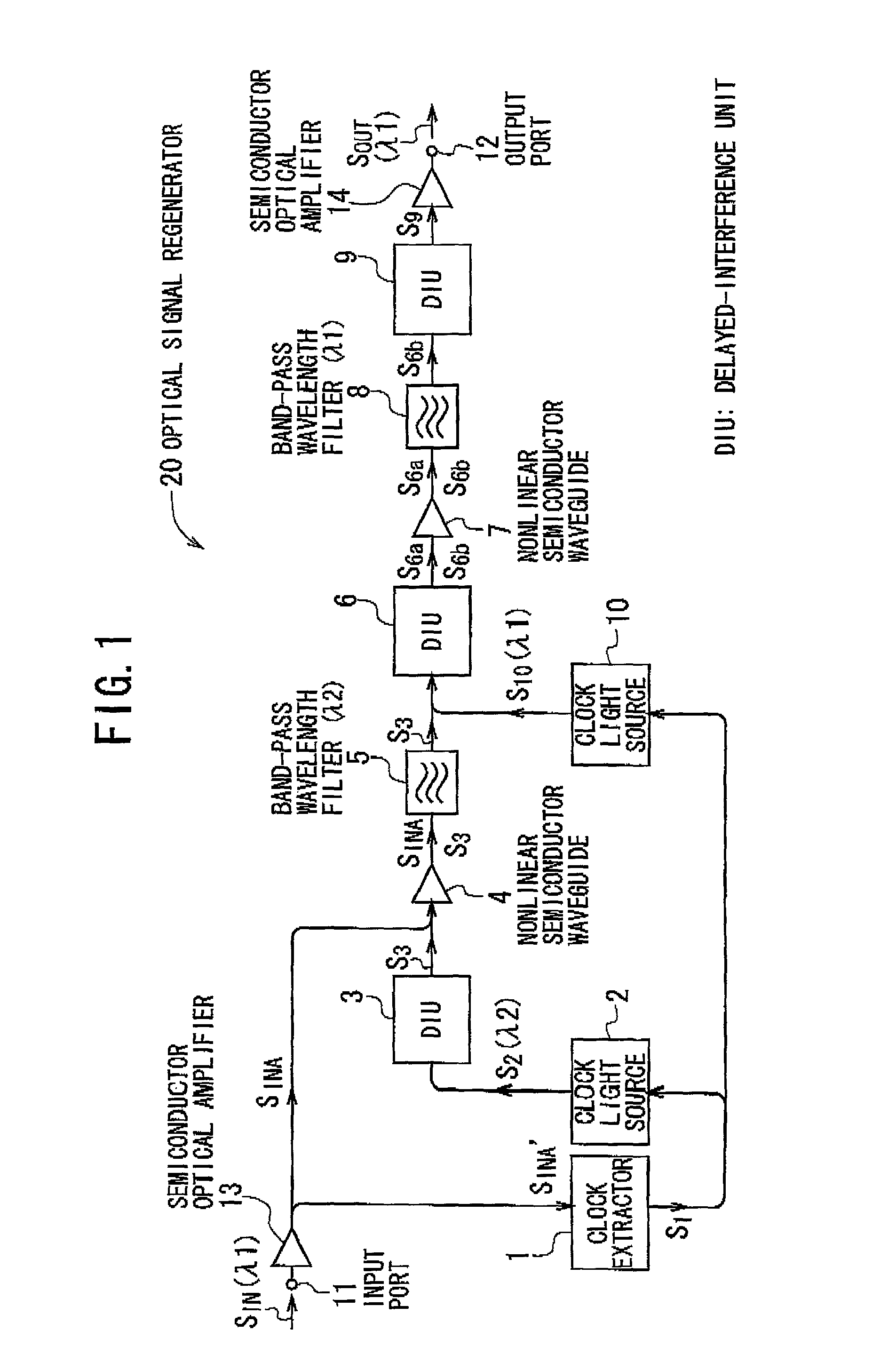
[0134]An all-optical signal regeneration system 20 according to a first embodiment of the invention has the configuration as shown in FIG. 1. This system 20 conducts the optical 3R repeating process in two steps.
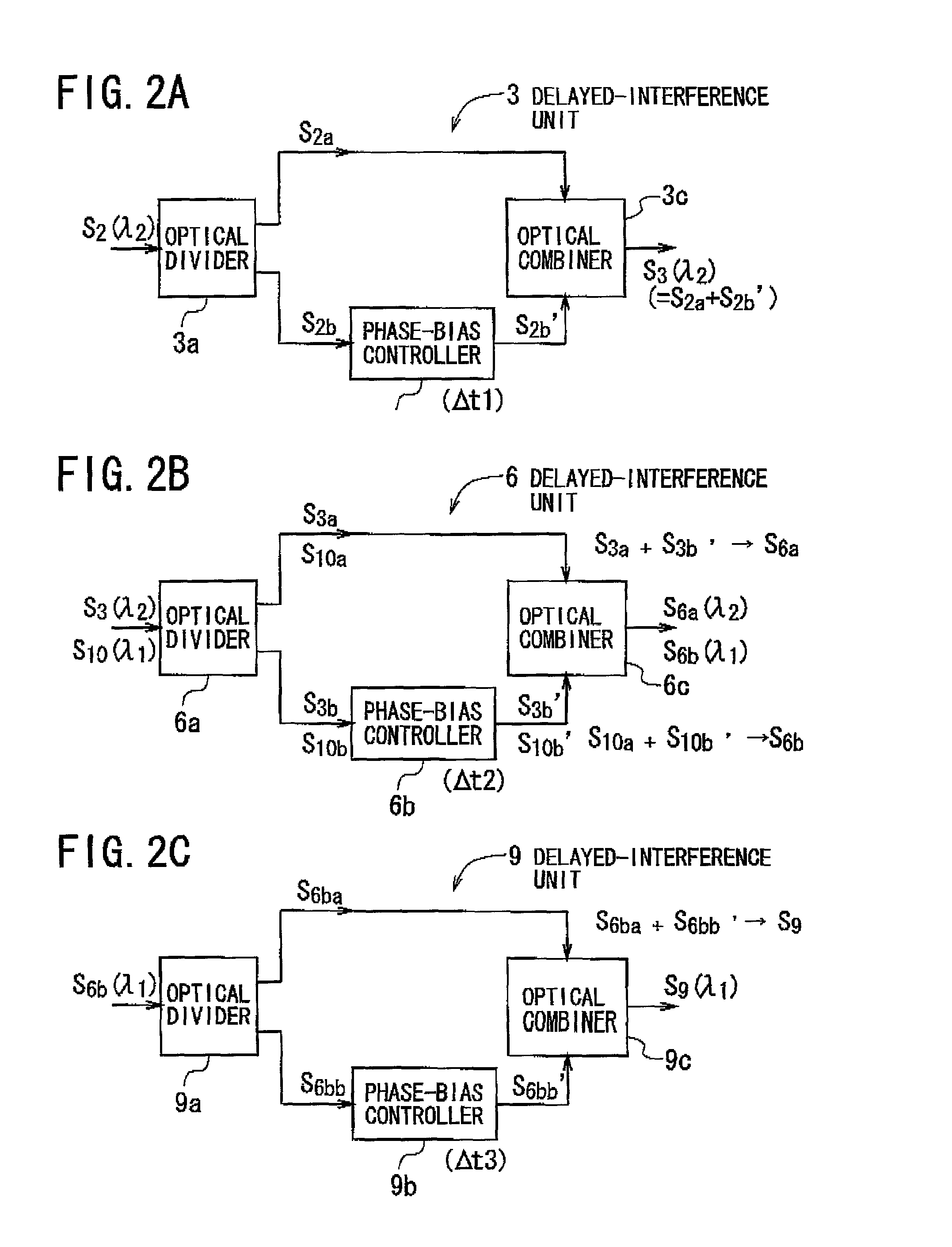
[0135]As shown in FIG. 1, the all-optical signal regeneration system 20 Comprises a clock extractor 1, a first clock light source 2, a first delayed-interference unit (DIU) 3, a first nonlinear semiconductor waveguide 4, a first bandpass wavelength filter 5, a second delayed-interference unit 6, a second nonlinear semiconductor waveguide 7, a second band-pass wavelength filter 8, a third delayed-interference unit 9, a second clock light source 10, an input port 11, an output port 12, a first semiconductor optical amplifier (SOA) 13, and a second semiconductor optical amplifier 14.
[0136]The first amplifier 13, the first interference unit 3, the first waveguide 4, the first filter 5, and the second interference unit 6 constitute the “first-stage optical 3R regeneration section...
second embodiment
[0193]FIG. 5 shows an all-optical signal regeneration system 60 according to a second embodiment of the invention. This system 60 provides the “optical 2R generation operation”, which is unlike the system 20 of the first embodiment.
[0194]As shown in FIG. 5, the all-optical signal regeneration system 60 comprises a first continuous-wave (CW) light source 41, a first nonlinear semiconductor waveguide 42, a first delayed-interference unit 43, a first band-pass wavelength filter 44, a second nonlinear semiconductor waveguide 45, a second delayed-interference unit 46, a second band-pass wavelength filter 47, a second CW light source 48, an input port 51, an output port 52, a first semiconductor optical amplifier (SOA) 53, and a second semiconductor optical amplifier 54.
[0195]The first amplifier 53, the first CW light source 41, the first waveguide 42, the first interference unit 43, and the first filter 44 constitute the “first-stage optical 2R regeneration section”. The second amplifier...
third embodiment
[0227]FIG. 9 shows an all-optical signal regeneration system 20A according to a third embodiment of the invention. This system 20A has the same configuration as the system 20 of the first embodiment except that the semiconductor optical amplifiers 13 and 14 are removed from the configuration of the system 20 of the first embodiment.
[0228]In the third embodiment, there is an additional advantage that the configuration of the system 20A is simplified, along with the same advantages as the system 20 of the first embodiment.
PUM
| Property | Measurement | Unit |
|---|---|---|
| repetition frequency | aaaaa | aaaaa |
| refractive index | aaaaa | aaaaa |
| refractive index | aaaaa | aaaaa |
Abstract
Description
Claims
Application Information


