
Optical waveguide with layered core and methods of manufacture thereof

a technology of optical waveguides and layered cores, applied in the direction of optical waveguide light guides, optical elements, instruments, etc., can solve the problems of partial loss of light transmission, signal degradation, or loss of entire signal

Inactive Publication Date: 2005-03-08
INTEL CORP
View PDF26 Cites 6 Cited by
  • Summary
  • Abstract
  • Description
  • Claims
  • Application Information

AI Technical Summary

Benefits of technology

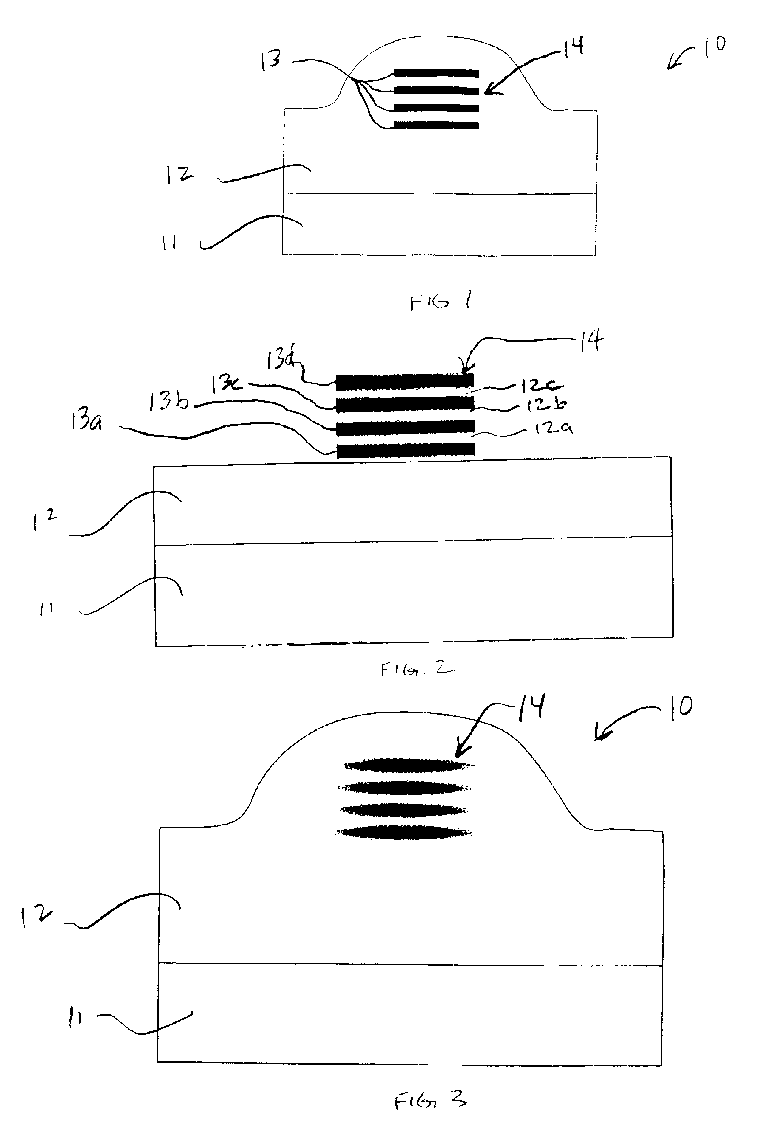
FIG. 3 is a sectional view of a waveguide manufactured in accordance with this disclosure after a cladding layer is been deposited on top of the stacked core and after the structure has been annealed to cause the stacked layers of the core to interdiffuse thereby reducing scattering caused by edge wall index perturbation;

Problems solved by technology

However, the differences in the index of refraction of the core and cladding also result in birefringence, or the separation of the light pulse or ray into two unequally refracted pulses or rays.
As a result, part of the light transmission is lost.
The majority of fiber optic telecommunications systems use standard single-mode silica fiber that does not preserve the polarization of the transmitted light.
If devices placed at any point in the fiber transmission path or at its end have response characteristics that depend on the polarization state of the light (i.e., polarization dependence), the signal may be degraded or lost altogether.

Method used


Image

  • Optical waveguide with layered core and methods of manufacture thereof
  • Optical waveguide with layered core and methods of manufacture thereof
  • Optical waveguide with layered core and methods of manufacture thereof

Examples


Embodiment Construction

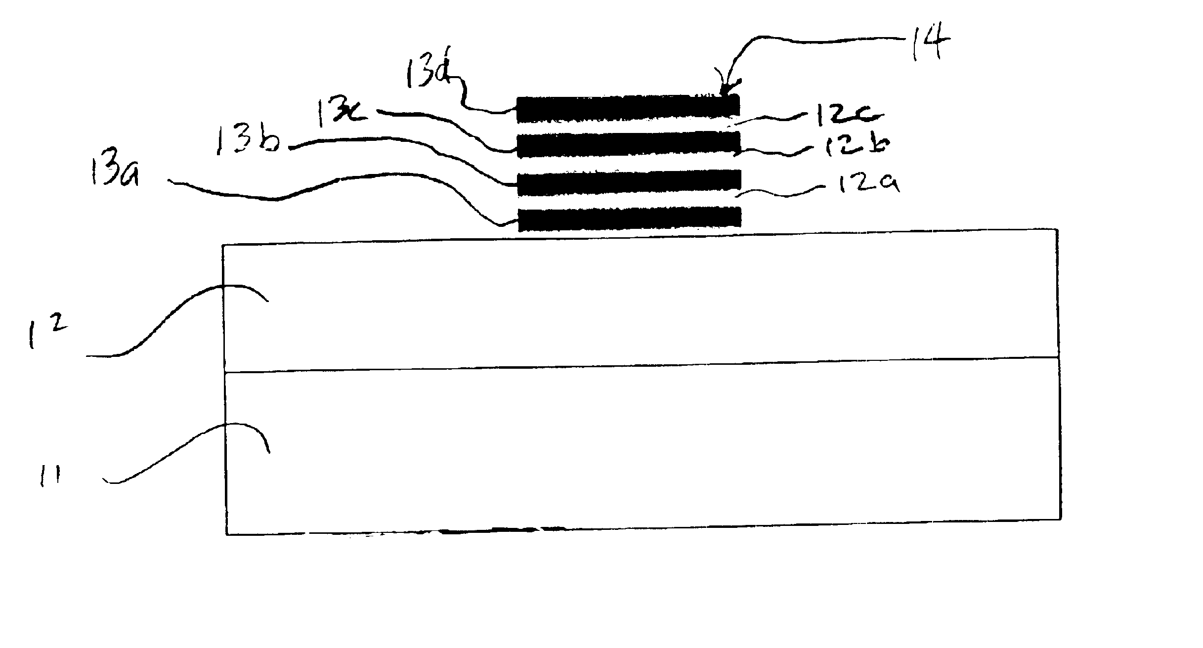
To provide an optical waveguide and other opto-electronic devices with reduced birefringence and reduced polarization dependence, waveguide and devices are made from binary systems of silica and silicon nitride. Using a plasma enhanced chemical vapor deposition (PECVD) process, a waveguide 10 having the structure illustrated in FIG. 1 is fabricated. The waveguide 10 includes a substrate 11 and a cladding 12. Embedded in the cladding 12 is a series of discreet layers 13 that form a core 14. Both the cladding 12 and the layers 13 of the core 14 comprise both silica and silicon nitride, or SiON. However, the cladding layer 12 has a lower nitrogen content that the discreet stacked layers 13 of the core 14. In the alternative, it is noted that the cladding 12 has a higher oxygen content than the discreet stacked layers 13 of the core 14.

To fabricate the waveguide 10 of FIG. 1, a cladding layer 12 is deposited on a substrate 11, preferably using a PECVD process using silane, nitrous oxide...


PUM

PropertyMeasurementUnit
spacingaaaaaaaaaa
temperaturesaaaaaaaaaa
temperatureaaaaaaaaaa

Abstract

A semiconductor waveguide is disclosed which includes a substrate coated with a cladding. A core is embedded in the cladding. The core includes a plurality of discreet stacked layers of core material surrounded by cladding material. The cladding and core layers each include silica and silicon nitride with the core layers having a higher nitrogen content than the cladding material. The core is fabricated by carefully manipulating the process parameters of a PECVD process.

Description

TECHNICAL FIELDSemiconductor opto-electronic devices including semiconductor optical waveguides and methods of manufacture thereof are disclosed.BACKGROUND OF THE RELATED ARTThere is a wide-ranging demand for increased communications capabilities, including more channels and greater bandwidth per channel. The needs range from long distance applications such as telecommunications between two cities to extremely short range applications such as the data-communications between two functional blocks (fubs) in a semiconductor circuit with spacing on the order of a hundred microns.Optical fibers can carry information encoded as optical pulses over long distances. The advantages of optical media include vastly increased data rates, lower transmission losses, lower basic cost of materials, smaller cable sizes, and almost complete immunity from stray electrical fields. Other applications for optical fibers include guiding light to awkward places (e.g., surgical applications), image guiding f...

Claims


Application Information

Patent Timeline
Patent Type & Authority Patents(United States)
IPC IPC(8): G02B6/13G02B6/12
CPCG02B6/131G02B2006/121G02B2006/12097
Inventor JOHANNESSEN, KJETIL
Owner INTEL CORP
Learn More