

Methods and apparatus for detecting and correcting reticle deformations in microlithography
a technology of reticle deformation and microlithography, which is applied in the field of microlithography, can solve the problems of distortion and deformation of the respective pattern portion, the current cpb microlithography technology does not yet embody a solution, and the pattern resolution limitation of optical microlithography has become a major limitation, and achieves the effect of greater accuracy
- Summary
- Abstract
- Description
- Claims
- Application Information
AI Technical Summary
Benefits of technology
Problems solved by technology
Method used
Image

Examples
Embodiment Construction
The invention is described below in the context of representative embodiments that are not intended to be limiting in any way. Also, certain aspects of the invention are described in connection with using an electron beam as an exemplary charged particle beam. It will be understood that the general principles described herein are applicable with equal facility to use of another type of charged particle beam, such as an ion beam, and to use of other lithographic-energy beams such as ultraviolet light or X-rays.
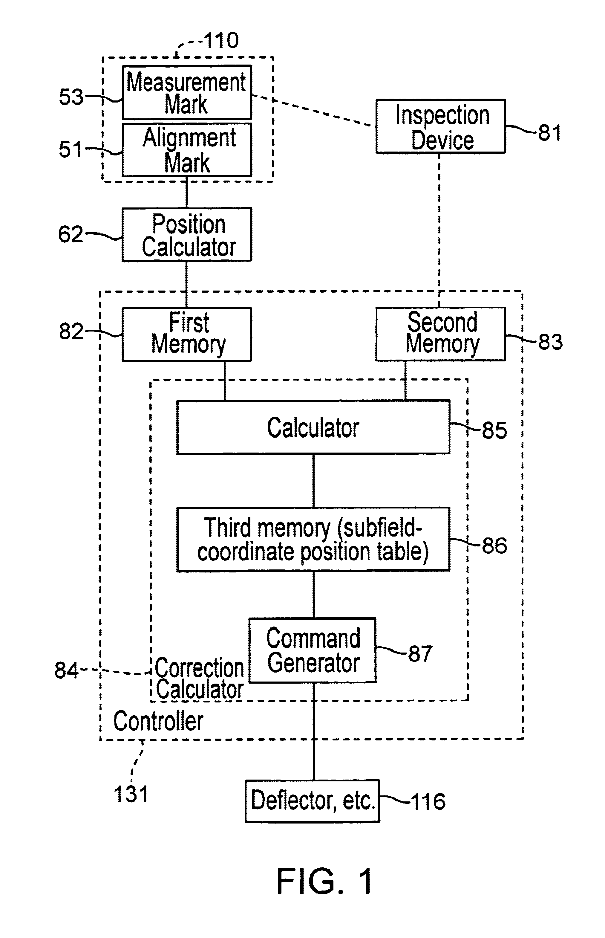
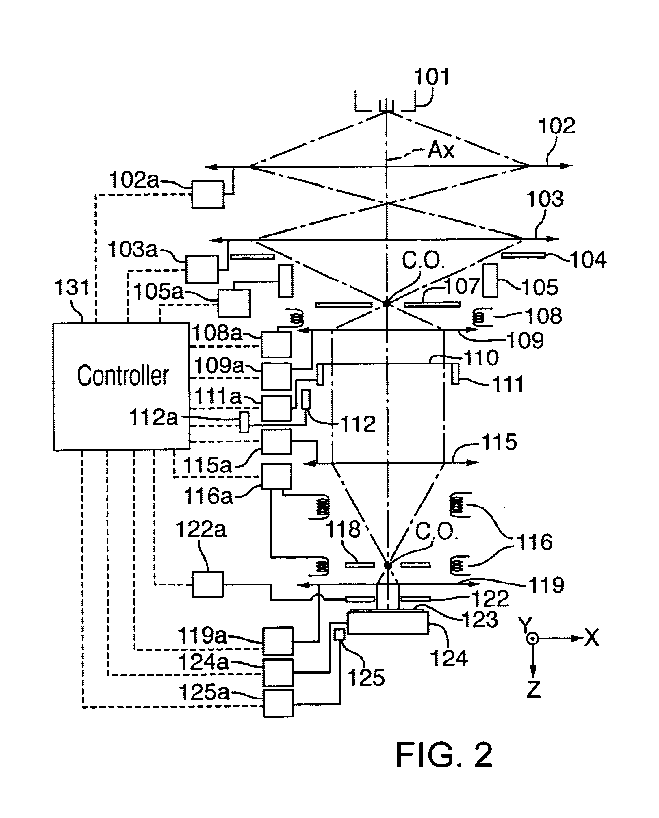
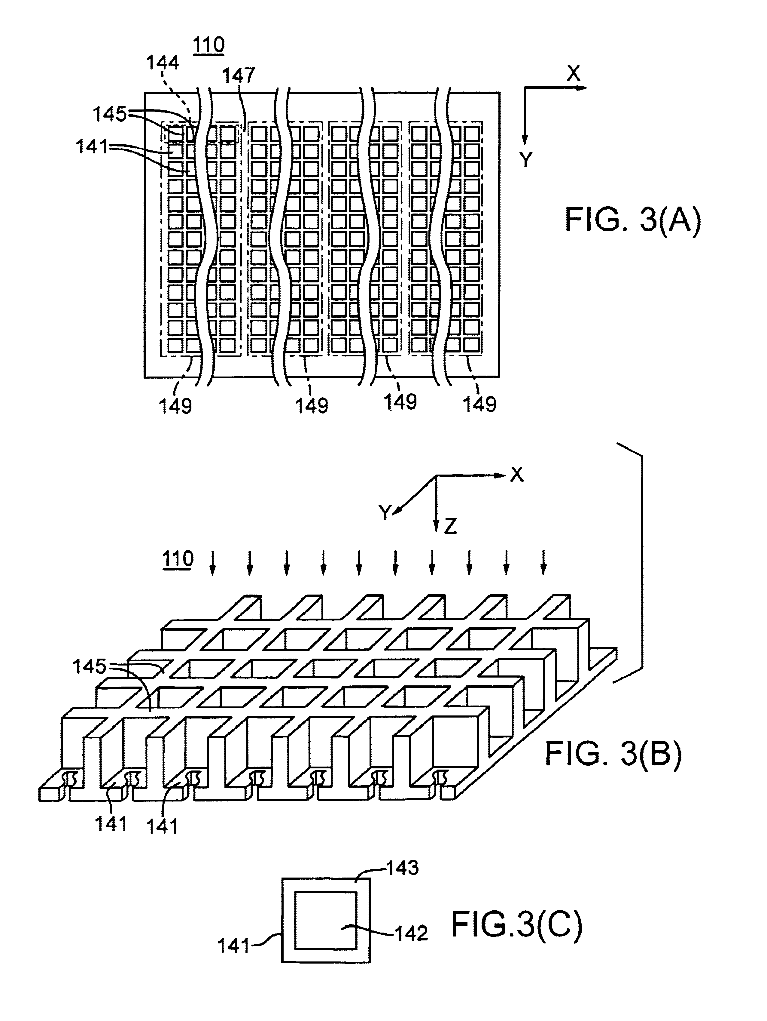
First, a general description of an electron-beam projection-exposure (microlithography) apparatus and method, employing a divided reticle, is provided below, referring to FIG. 2. FIG. 2 also depicts general imaging and control relationships of the subject system.
Situated at the extreme upstream end of the system is an electron gun 101 that emits an electron beam propagating in a downstream direction generally along an optical axis Ax. Downstream of the electron gun 101 are a fi...
PUM
 Abstract
Description
Claims
Application Information