Electrical through wafer interconnects

a technology of wafers and interconnects, applied in the field of electric through wafer interconnects, can solve the problems of addressing individual array elements, limiting the dynamic range and frequency bandwidth of the device array, and requiring significant sacrifice of array element area, etc., and achieves the effect of low parasitic capacitance and resistan

Inactive Publication Date: 2004-12-28
THE BOARD OF TRUSTEES OF THE LELAND STANFORD JUNIOR UNIV
View PDF5 Cites 81 Cited by
  • Summary
  • Abstract
  • Description
  • Claims
  • Application Information

AI Technical Summary

Benefits of technology

It is a further object of the present invention to provide a wafer which includes front side and back side pads and a through wafer interconnect with low parasitic capacitance and resistance.

Problems solved by technology

One of the main problems in fabricating two dimensional arrays is that of addressing the individual array elements.
If the array size is large, a significant sacrifice in the array element area is required if the addressing is done through a routing network on the top side of the substrate.
The interconnect between the array elements and their electronics gives rise to parasitic capacitance which limits the dynamic range and frequency bandwidth of the device array.
However, integrating the devices, the electronics and the interconnects on the same wafer leads to a compromise in the performance of both the electronics and the device array.

Method used


Image

  • Electrical through wafer interconnects
  • Electrical through wafer interconnects
  • Electrical through wafer interconnects

Examples


Embodiment Construction

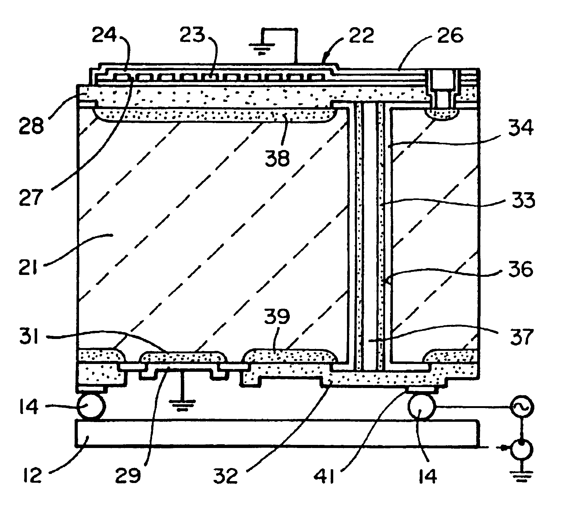
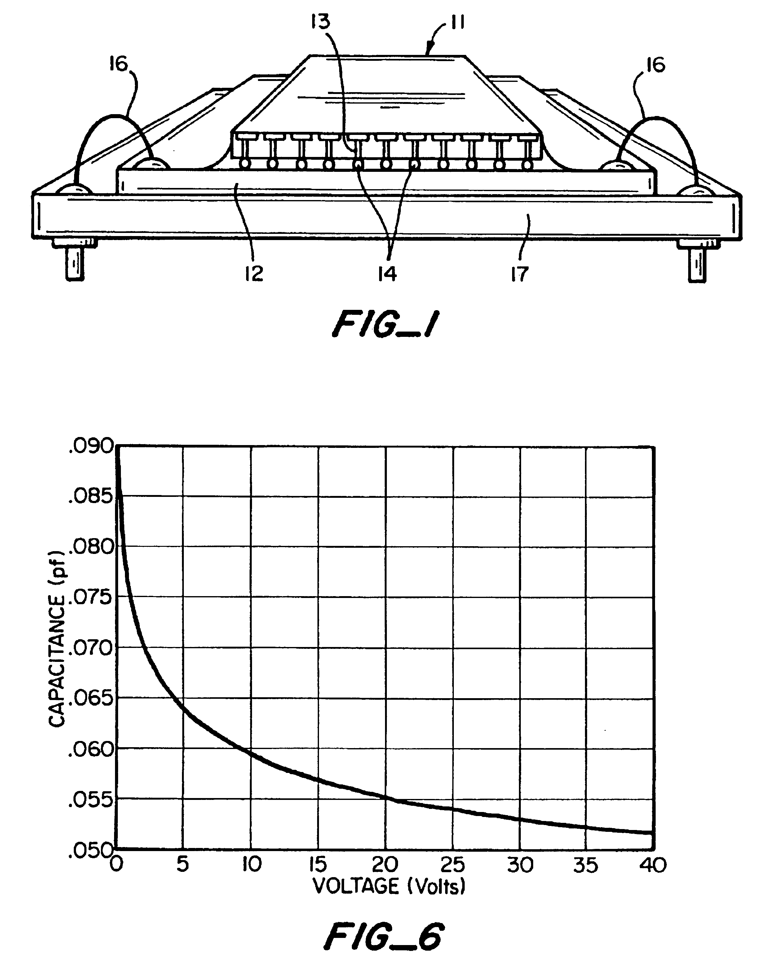
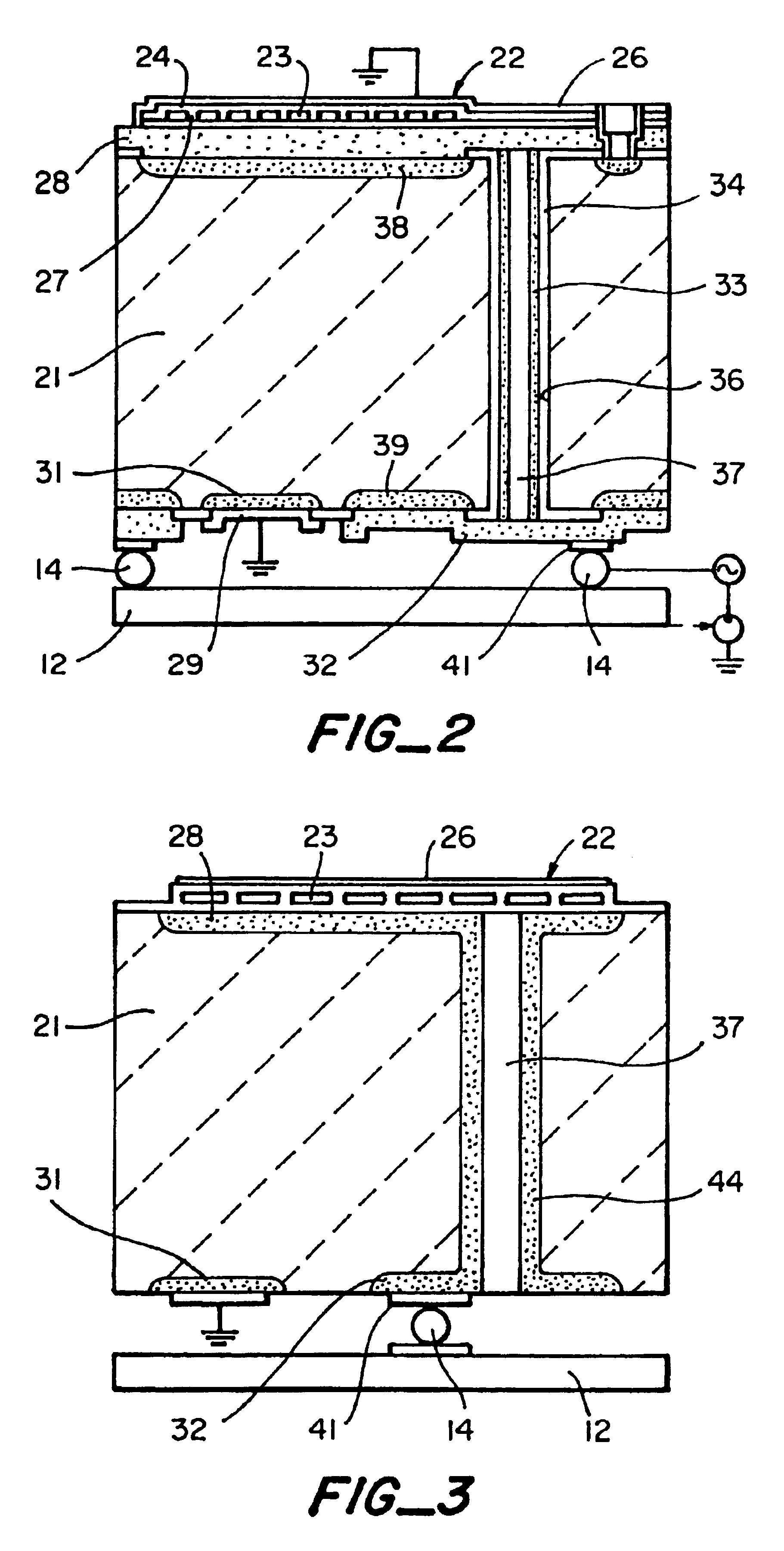
FIG. 1 shows MEMS devices 11 connected to integrated circuits 12 with through wafer interconnects 13 and solder bumps 14. The integrated circuit (electronics) 12 is shown wire bonded 16 to a printed circuit board 17. The MEMS array is connected with the electronic circuits without sacrificing the performance of either one and minimizing the parasitic capacitance. In transducer array operation the parasitic capacitance of the interconnect between an array element and its electronics is the limiting factor for the dynamic range and frequency bandwidth. Therefore, it is always best to put the electronics as close to the array elements as possible. To do this, an electrical through wafer interconnect (ETWI) is employed to address the array elements individually, where the front side of the wafer is fully populated with the array elements and the backside is solely dedicated to bond pads for the flip-chip bonding to the printed circuit board (PCB) or the integrated circuits as shown in F...


PUM


Abstract

A wafer with through wafer interconnects. The wafer includes spaced through wafer vias which extend between the back side and front side of the wafer. A conductor within each of said vias connects to front and back side pads. Functions associated with said conductor and said pads provide a depletion region in the wafer between the pads and wafer or pads and conductor and the wafer.

Description

This invention relates generally to electrical through wafer interconnects and more particularly to through wafer interconnects in which the parasitic capacitance is minimized.In co-pending application Ser. No. 09 / 667,203 filed Sep. 21, 2000, there is described an ultrasonic transducer with through wafer connections. Capacitive micro machined ultrasonic transducer arrays include membranes which are supported on the front side of a substrate or wafer by isolator supports such as silicon nitride, silicon oxide and polyimide. Transducers of this type are described, for example, in U.S. Pat. Nos. 5,619,476; 5,870,351; and 5,894,452. Micromachined two-dimensional arrays of droplet ejectors which include a flexible membrane supported on a substrate are described, for example, in U.S. Pat. No. 6,474,786. Other two-dimensional device arrays such as for example, arrays of vertical cavity surface emitting lasers, mirrors, piezoelectric transducers, photo detectors and light emitting diodes ar...

Claims


Application Information

Patent Timeline
Patent Type & Authority Patents(United States)
IPC IPC(8): B06B1/06B06B1/02
CPCB06B1/0292B06B1/06H01L21/76898H01L2224/48227H01L2924/12041H01L2924/10253H01L2924/12032H01L2924/00
Inventor CHENG, CHING-HSIANGERGUN, ARIF S.KHURI-YAKUB, BUTRUS T.
Owner THE BOARD OF TRUSTEES OF THE LELAND STANFORD JUNIOR UNIV
Why Eureka
Try Eureka