High sensitivity snap shot CMOS image sensor

a high-sensitivity, image sensor technology, applied in the direction of pulse technique, radiation control device, optical radiation measurement, etc., can solve the problems of affecting the quality of snap shots is not high, so as to achieve the effect of saving power and higher clock ra

Inactive Publication Date: 2005-01-04
ESS TECH INT INC +1
View PDF4 Cites 64 Cited by
  • Summary
  • Abstract
  • Description
  • Claims
  • Application Information

AI Technical Summary

Benefits of technology

A CMOS imager system with a variable frame rate can be employed to accommodate very high frame rates (>60 FPS) for digital still applications to freeze motion, and lower frame rates (˜30 FPS) for viewfinder or motion picture application. The variable frame rate saves power during continuous operation as the high frame rate for digital still application is employed only during the capture of a still picture at high shutter speed. Preferably,

Problems solved by technology

In CCD solid-state image sensors, the amplifier noise generally becomes dominant when 30 frames per second (FPS) is employed for image sizes over several hundred thousand pixels.
Unfortunately, because video images are not generally of the highest quality, the snap shot of the still image will also not be of the highest quality.
Such snap shots are especially inferior when compared with typical still i

Method used


Image

  • High sensitivity snap shot CMOS image sensor
  • High sensitivity snap shot CMOS image sensor
  • High sensitivity snap shot CMOS image sensor

Examples


Embodiment Construction

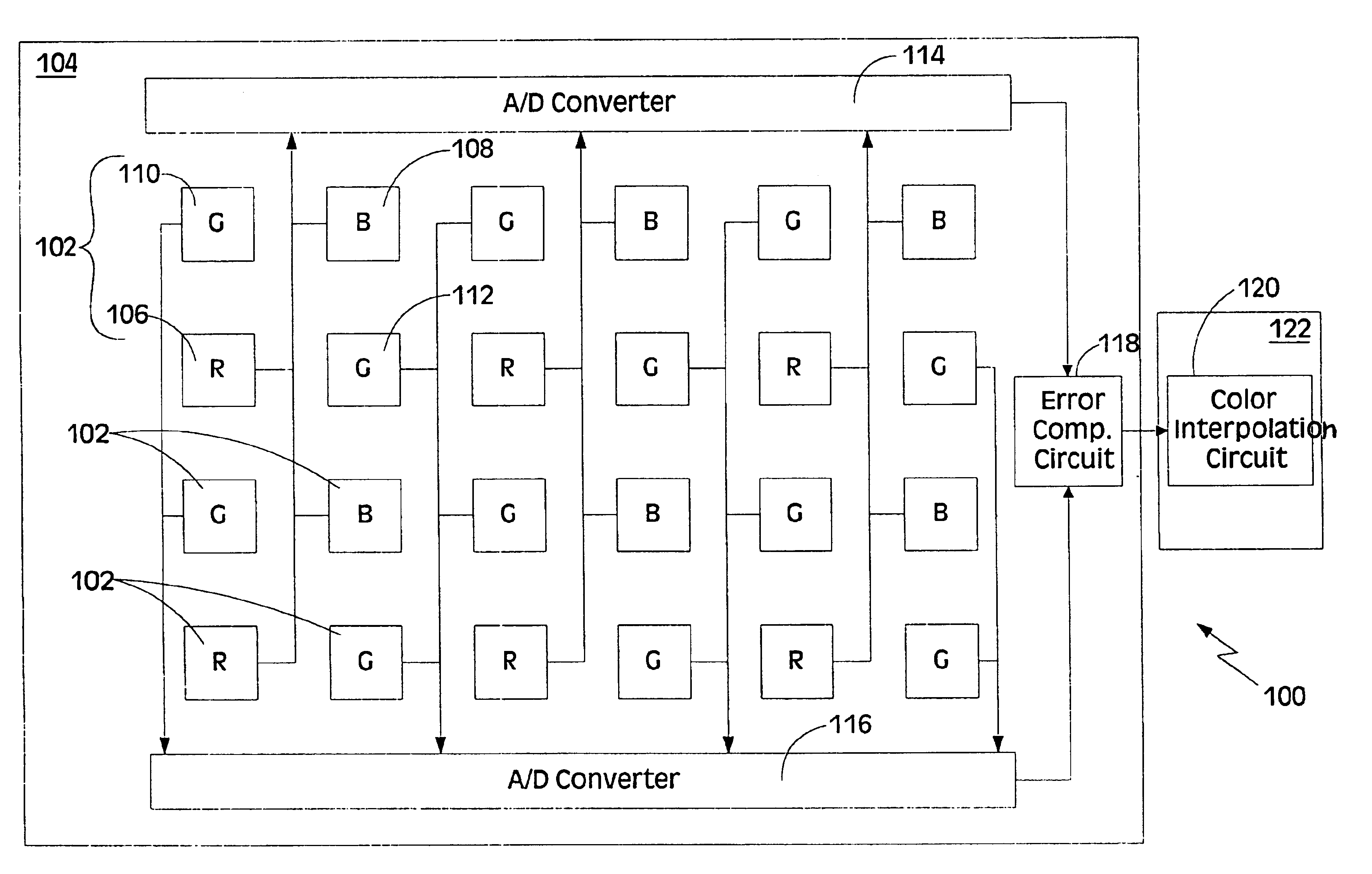
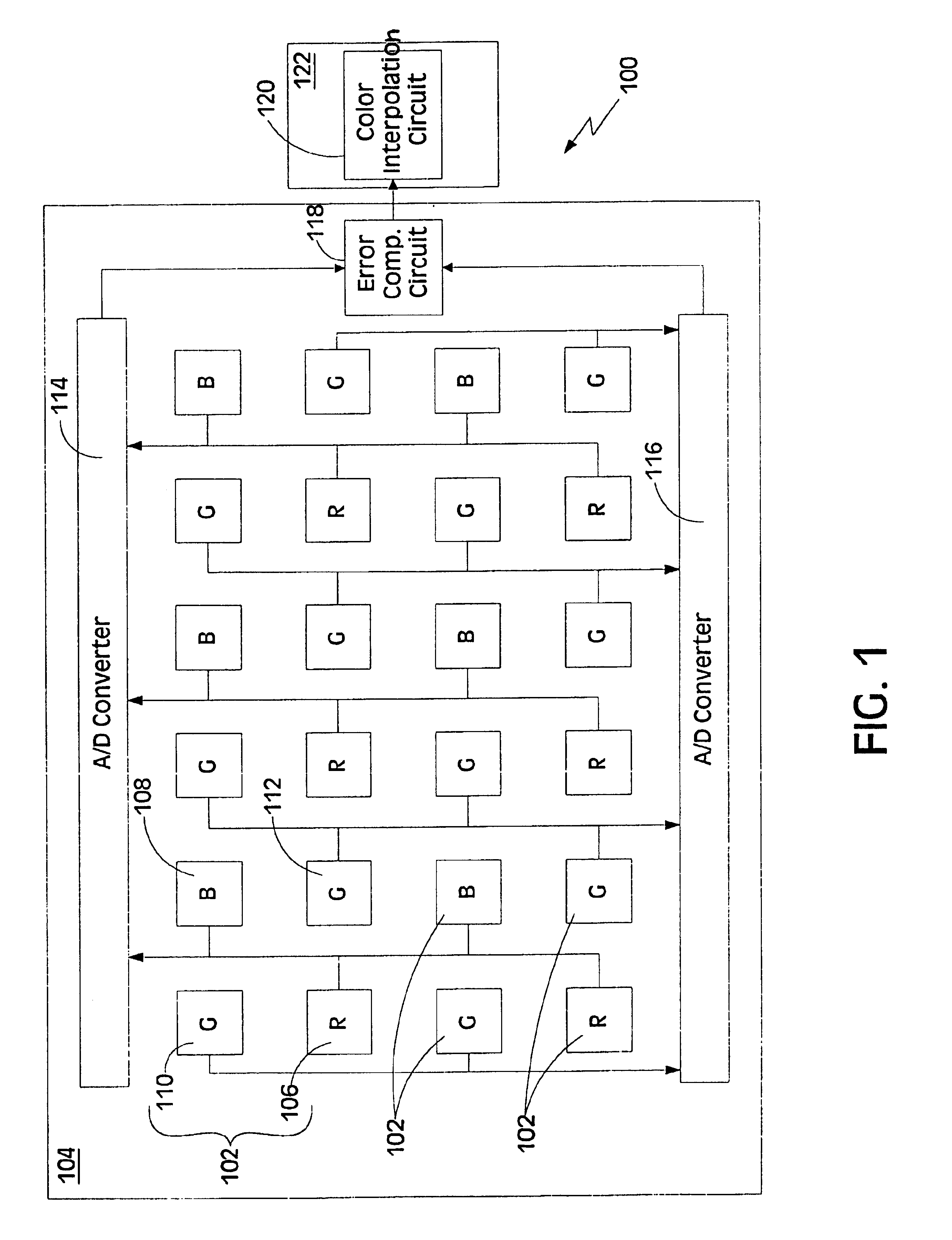
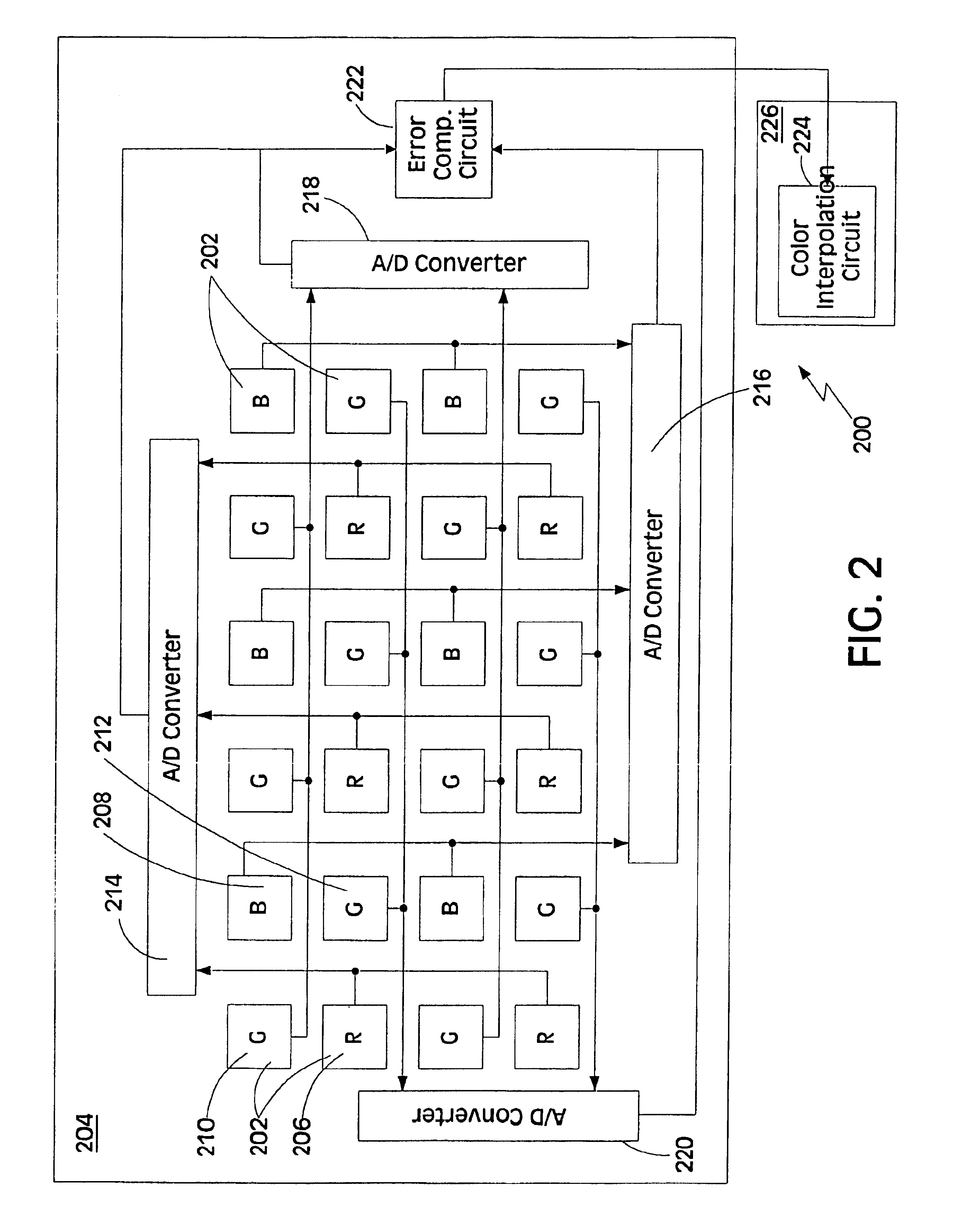
FIG. 1 illustrates a solid state imaging device 100 in accordance with the present invention. The imaging device 100 comprises a two-dimensional array of image pixels 102 disposed on a chip 104 using four color channels (one red, one blue and two greens) to define a color image. Each pixel 102 is either a red pixel 106 having a red photodiode, a blue pixel 108 having a blue photodiode or a green pixel 110, 112 having a green photodiode. The standard approach uses identical photodiode construction for each of the sensing elements. The green photodiode responds to green light since only green light is allowed to strike the photodiode through the filter element. In a similar manner, a preferential response is created to blue and red light.

The output of each pixel 102 is a signal proportional to the amount of light incident on the pixel 102. Accordingly, the output of the red pixel 106 is a signal proportional to the amount of red light incident on the pixel 106. Similarly, the output o...


PUM


Abstract

The present invention is directed to a solid state imaging device comprising a red pixel, a blue pixel, a first green pixel, a second green pixel, two analog-to-digital converters and a color interpolation circuit. The first analog-to-digital converter converts the output of the red pixel and output of the blue pixel into digital signals. The second analog-to-digital converter converts the output of the first green pixel and output of the second green pixel into digital signals. The color interpolation circuit combines the digital signals to determine the color of the pixel.
The solid state imaging device may further comprise a third analog-to-digital converter, a fourth analog-to-digital converter, a programmable clock generator and a control. The third analog-to-digital converter converts the output of the blue pixel into a digital signal and the fourth analog-to-digital converter converts the output of the second green pixel into a digital signal. The programmable clock generator has a first clock frequency and a second clock frequency, where the first clock frequency is slower than the second clock frequency. The control is coupled to the programmable clock generator, the third analog-to-digital converter and the fourth analog-to-digital converter. The control deactivates the third and fourth analog-to-digital converters if the programmable clock generator is at the first clock frequency, and the control activates the third and fourth analog-to-digital converters if the programmable clock generator is at the second clock frequency.

Description

TECHNICAL FIELDThis invention relates generally to solid-state imaging devices such as Complementary Metal Oxide Semiconductor (“CMOS”) solid-state imagers. More particularly the invention relates to a solid-state imaging device implementing multiple analog-to-digital (“A / D”) converters to obtain high frame rates.BACKGROUND OF THE INVENTIONSolid-state image sensors (also known as “image sensors,”“imagers,” or “solid-state imagers”) have broad applications in many areas including commercial, consumer, industrial, medical, defense and scientific fields. Solid-state image sensors convert a received image such as from an object into a signal indicative of the received image. Examples of solid-state image sensors including charge coupled devices (“CCD”), photodiode arrays, charge injection devices (“CID”), hybrid focal plane arrays and complementary metal oxide semiconductor (“CMOS”) imaging devices.Solid-state image sensors are fabricated from semiconductor materials (such as silicon or...

Claims


Application Information

Patent Timeline
IPC IPC(8): H01L27/00H01L27/146
CPCH01L27/14645H01L27/14621H04N25/78H04N25/134
Inventor MANN, RICHARD A.
Owner ESS TECH INT INC
Why Eureka
Try Eureka