Light emitting diode
a technology of light-emitting diodes and diodes, which is applied in the direction of basic electric elements, electrical equipment, and semiconductor devices, etc., can solve the problems of many problems, many technical bottlenecks cannot be overcome, and no major breakthrough, etc., to achieve good heat dissipation, broaden the application range of chips, and increase the sustainable power during operation.
- Summary
- Abstract
- Description
- Claims
- Application Information
AI Technical Summary
Benefits of technology
Problems solved by technology
Method used
Image

Examples
first embodiment
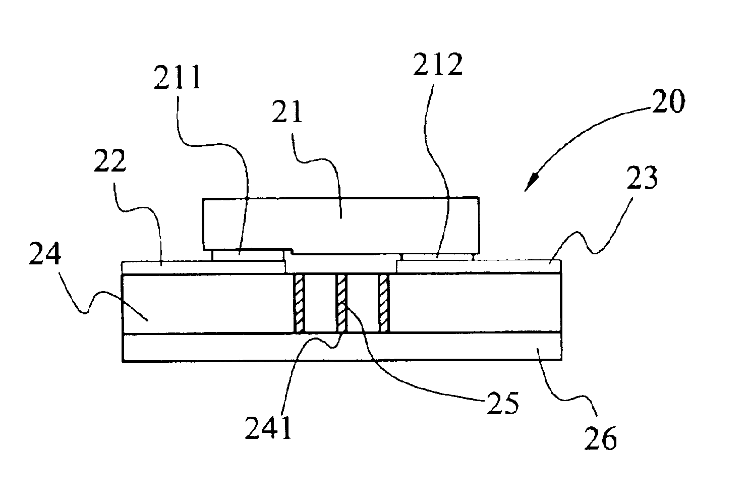
Please refer to FIG. 4 for the invention, which adds a metal heat dissipating layer 26 below the heat dissipating substrate 24 of the light emitting chip 20. This metal heat dissipating layer 26 is composed of gold, silver, tin, or any or all of their alloys. It allows fast heat dissipation and uses the metal dissipating layer 26 as the medium for the die binding process for attaching the frame of the LED.
second embodiment
Please refer to FIG. 5 for the second embodiment, which applies the invention as the light source of the LED. After the light emitting chip is packaged, it forms the LED 30 shown in the illustration. The light emitting chip 20 is attached inside the groove 311 of the frame 31. After securing the chip, it is then wire bonded so the p-electrode 22 of the light emitting chip 20 is electrically connected to the frame 31, and the n-electrode 23 is electrically connected to the frame 32. Finally, epoxy resin 33 is used to seal the packaging to form the LED 30 shown in the illustration. Using the conducting cylinders 25 on the emitting structure of the light emitting chip of the invention, the heat energy of the LED can be well dissipated after the chip is electrically connected. As shown in the illustration, the bottom of the heat dissipated substrate 24 is connected to the bottom of groove 311 of frame 31, so each of the conducting cylinders 25 of the heat dissipating substrate 24 is als...
third embodiment
Please refer to FIG. 6 for an illustration of the invention, which packages the invention into a color mixing wavelength LED 40. As shown in the illustration, the light emitting chip 20 disclosed by the invention is secured in the groove 411 of the frame 41 and then wired so the p-electrode 22 of the light emitting chip 20 is electrically connected to the frame 41, and the n-electrode 23 is electrically connected to the frame 42. After the wiring process, a light hybrid layer 43 covers the light emitting chip 20 completely inside the groove 441. Once electricity flows through, the light generated by the light emitting chip 20 illuminates the light hybrid layer 43 and excites the different materials in the light hybrid layer 43 to change the wavelength, and outputs a light of mixed color. The light hybrid layer is composed of a mixture of scattering particles, fluorescent particles and diffracting particles. The materials for the scattering particles are quartz, glass, or other trans...
PUM
 Abstract
Description
Claims
Application Information
 - R&D
- Intellectual Property
- Life Sciences
- Materials
- Tech Scout
- Unparalleled Data Quality
- Higher Quality Content
- 60% Fewer Hallucinations
Browse by: Latest US Patents, China's latest patents, Technical Efficacy Thesaurus, Application Domain, Technology Topic, Popular Technical Reports.
© 2025 PatSnap. All rights reserved.Legal|Privacy policy|Modern Slavery Act Transparency Statement|Sitemap|About US| Contact US: help@patsnap.com