Light emitting device having a dopant in a light emitting layer and method of producing the light emitting device

a light emitting device and light emitting layer technology, applied in the direction of discharge tube luminescnet screen, other domestic articles, natural mineral layered products, etc., can solve the problems of low charge injecting and charge transporting properties, loss of light emitting efficiency of the device, and difficulty in causing a large current, etc., to achieve low-voltage drive, high efficiency, and high luminance

Inactive Publication Date: 2005-01-04
CANON KK
View PDF4 Cites 43 Cited by
  • Summary
  • Abstract
  • Description
  • Claims
  • Application Information

AI Technical Summary

Benefits of technology

In consideration of the drawbacks in the conventional technologies explained in the foregoing, the object of the present invention is to provide an organic

Problems solved by technology

Among such phosphorescent materials, there are known ones with low charge injecting and charge transporting properties, in which it is difficult to cause a large current at a low voltage.
Also many organic materials are known to form a cluster of plural molecules at the evaporation, and the light emitting layer involving su

Method used


Image

  • Light emitting device having a dopant in a light emitting layer and method of producing the light emitting device
  • Light emitting device having a dopant in a light emitting layer and method of producing the light emitting device
  • Light emitting device having a dopant in a light emitting layer and method of producing the light emitting device

Examples


example 1

A device was prepared by employing CBP as the host material of a light emitting layer and doping the light emitting layer with the Ir complex C as the light emitting material at a concentration of 7 wt. % and with the Ir complex A as the light emitting compound at a concentration of 3 wt. %. The employed Ir complex A has a function of increasing the current in the device, thus also serving as the current enhancing material.

example 2

A device was prepared by employing CBP as the host material of the light emitting layer, and doping the region of a thickness of 10 nm at the side of the hole transport layer within the light emitting layer of a thickness of 40 nm, with the Ir complex C as the light emitting material at a concentration of 7 wt. % and with the Ir complex A as the light emitting compound at a concentration of 3 wt. %, while co-evaporating the Ir complex C alone at a concentration of 7 wt. % in the remaining 30 nm region. The employed Ir complex A has a function of increasing the current in the device, thus also serving as the current enhancing material.

Table 2 shows the results of measurement of current and luminance of the above-described device and the device of the comparative example 11 under the application of a DC voltage of 10 V.

TABLE 2Current (mA / cm2)Luminance (cd / m2)Example 223.5621Comp. Ex. 1111.8426

The results in Table 2 confirm that the device of the example 2 showed an increase in the cur...
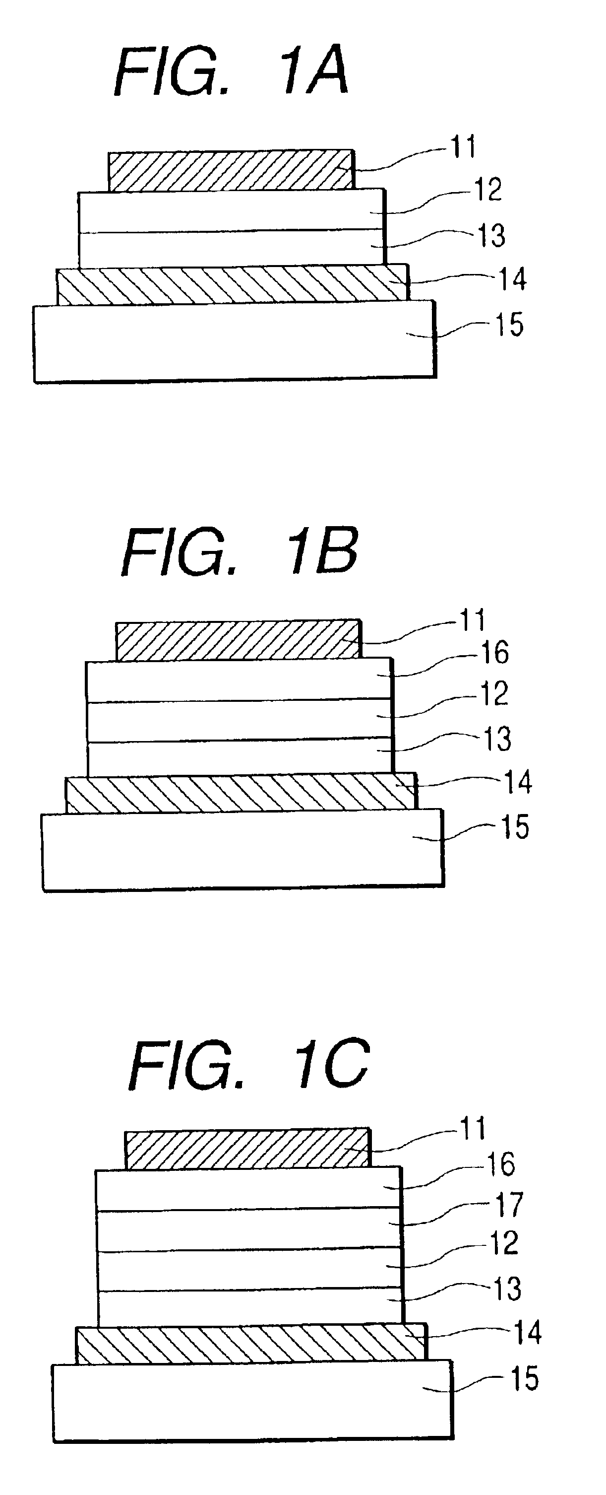
example 3

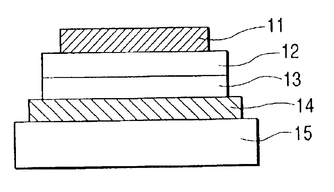
In this example, there was employed a device configuration with a four-layered organic layer as shown in FIG. 1C. An ITO film (transparent electrode 14) of a thickness of 100 nm was patterned on a glass substrate (transparent substrate 15). On thus prepared ITO substrate, following organic layers and electrode layers were formed in succession by vacuum evaporation by resistance heating in a vacuum chamber of 10−4 Pa:

Hole transport layer 13 (40 nm): FL03 (following chemical formula)

Light emitting layer 12 (40 nm): host material+light emitting material 1+light emitting material 2

Electron transport layer 17 (50 nm): Bphen (following chemical formula)

Electron injection layer 16 (1 nm): KF

Metal electrode layer (100 nm): Al

It was so patterned that the electrodes had an opposed area of 3 mm2.

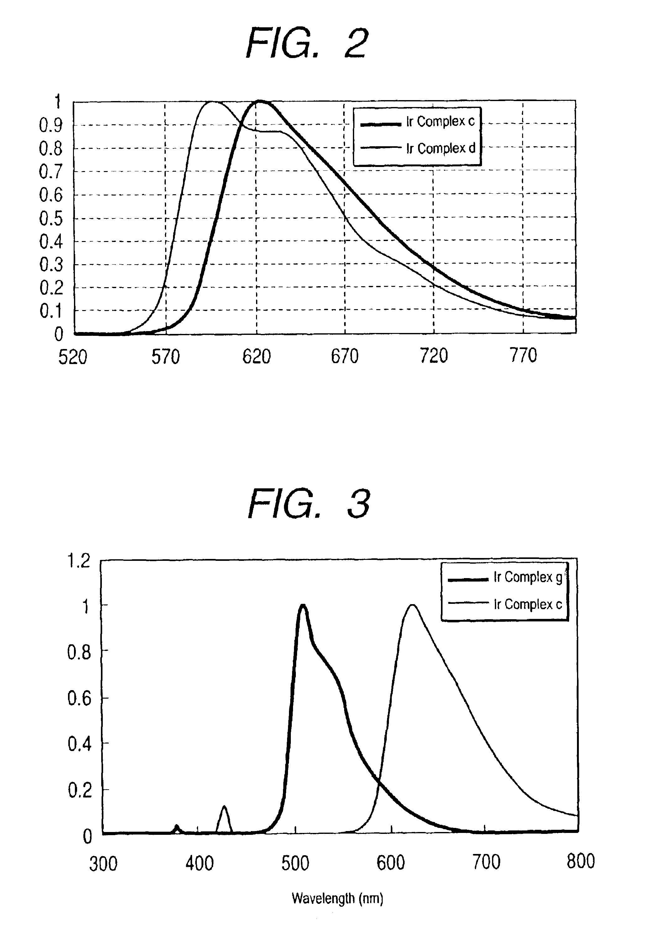
In forming the light emitting layer 12, the Ir complex C was employed as the light emitting material 1, and the Ir complex D was employed as the light emitting material 2.

(Ir Complex D)

The Ir comple...


PUM

PropertyMeasurementUnit
Timeaaaaaaaaaa
Timeaaaaaaaaaa
Timeaaaaaaaaaa

Abstract

A light emitting device having an anode and a cathode provided on a substrate, and an organic light emitting layer between the anode and the cathode, where the organic light emitting layer includes a light emitting material and a dopant for improving the dispersibility thereof. As the dopant, there are employed a light emitting compound and a non-light emitting compound or a current enhancing material. In case of employing the light emitting compound, the composition corresponds to a case of utilizing plural light emitting materials, and, in such case, the light emission wavelengths are preferably mutually closer. Also, evaporation of the light emitting material and the dopant in the same evaporation boat makes it possible to reduce evaporation temperature, thereby improving the dispersability of the light emitting material.

Description

BACKGROUND OF THE INVENTION1. Field of the InventionThe present invention relates to a light emitting device utilizing an organic compound, and more detailedly to a light emitting device, particularly an organic electroluminescent device (organic EL device), having excellent luminance, efficiency and drive durability by doping a light emitting layer with plural compounds.2. Related Background ArtThe organic EL device is being actively investigated for its applications as a light emitting device capable of showing a high speed response and a high efficiency. The basic configuration of such device is shown in FIGS. 1A, 1B and 1C (for example see. Macromol. Symp., 125, 1-48(1997)).As shown in FIGS. 1A, 1B and 1C, the organic EL device is generally composed, on a transparent substrate 15, of a transparent electrode 14, a metal electrode 11, and an organic layer sandwiched therebetween and consisting of plural organic films.In the configuration shown in FIG. 1A, the organic layer consist...

Claims


Application Information

Patent Timeline
IPC IPC(8): C09K11/06H01L51/50H01L51/05H01L51/30H01L51/00
CPCC09K11/06H01L51/0058H01L51/0059H01L51/006H01L51/0085H01L51/0094H01L51/5012H01L51/5016H01L51/5052H05B33/14Y10S428/917C09K2211/1003C09K2211/1007C09K2211/1011C09K2211/1014C09K2211/1018C09K2211/1029C09K2211/1048C09K2211/1059C09K2211/1092C09K2211/1096C09K2211/18C09K2211/185H01L51/0051H01L51/0053H01L51/0081H01L2251/308C09K2211/10H10K85/611H10K85/621H10K85/631H10K85/626H10K85/633H10K85/324H10K85/342H10K85/40H10K50/11H10K2101/10H10K2102/103
Inventor FURUGORI, MANABUOKADA, SHINJIROTSUBOYAMA, AKIRATAKIGUCHI, TAKAOMIURA, SEISHIMORIYAMA, TAKASHIIGAWA, SATOSHIKAMATANI, JUNIWAWAKI, HIRONOBU
Owner CANON KK
Why Eureka
Try Eureka