Clocked based method and devices for measuring voltage-variable capacitances and other on-chip parameters

a voltage-variable capacitance and clock-based technology, applied in the testing/measurement of individual semiconductor devices, semiconductor/solid-state devices, instruments, etc., can solve the problems of increasing unreliability of measurement, inaccurate and unreliability, and cumbersome metering

Inactive Publication Date: 2005-01-04
MONTEREY RES LLC
View PDF1 Cites 80 Cited by
  • Summary
  • Abstract
  • Description
  • Claims
  • Application Information

AI Technical Summary

Benefits of technology

By way of introduction only, the embodiments illustrated herein disclose methods and apparatus for measuring device parameters such as capacitances including voltage variable capacitances. A test circuit allows the current and voltage characteristics of the device parameter to be measured while excluding parasitic effects. A bias voltage is vari

Problems solved by technology

Such measurements have grown increasingly unreliable and difficult to make as integrated circuit dimensions have decreased.
However, such a meter can be cumbersome, inaccurate and unreliable.
Although most on-chip capacitances of interest could be represented in test chip test structures, the large sizes of such structures often prevent their use.
Achieving capacitance measurement structures that have enough capacitance to make accurate measurements possible requires that the structures be very large.
These large structures consume inordinate amounts of valuable test chip space.
Due to each stepper's optical constraints, the area of a wafer or exposure field that a stepper can pattern in a single exposure is limited.
Changing reticules requires that a stepper be disabled for a significant period of time.
Any such stepper “down time” is prohibitively costly.
It would be very impractical, for example, to use one reticule to pattern a layer on a portion of the wafers in a wafer lot and to then

Method used


Image

  • Clocked based method and devices for measuring voltage-variable capacitances and other on-chip parameters
  • Clocked based method and devices for measuring voltage-variable capacitances and other on-chip parameters
  • Clocked based method and devices for measuring voltage-variable capacitances and other on-chip parameters

Examples


Embodiment Construction

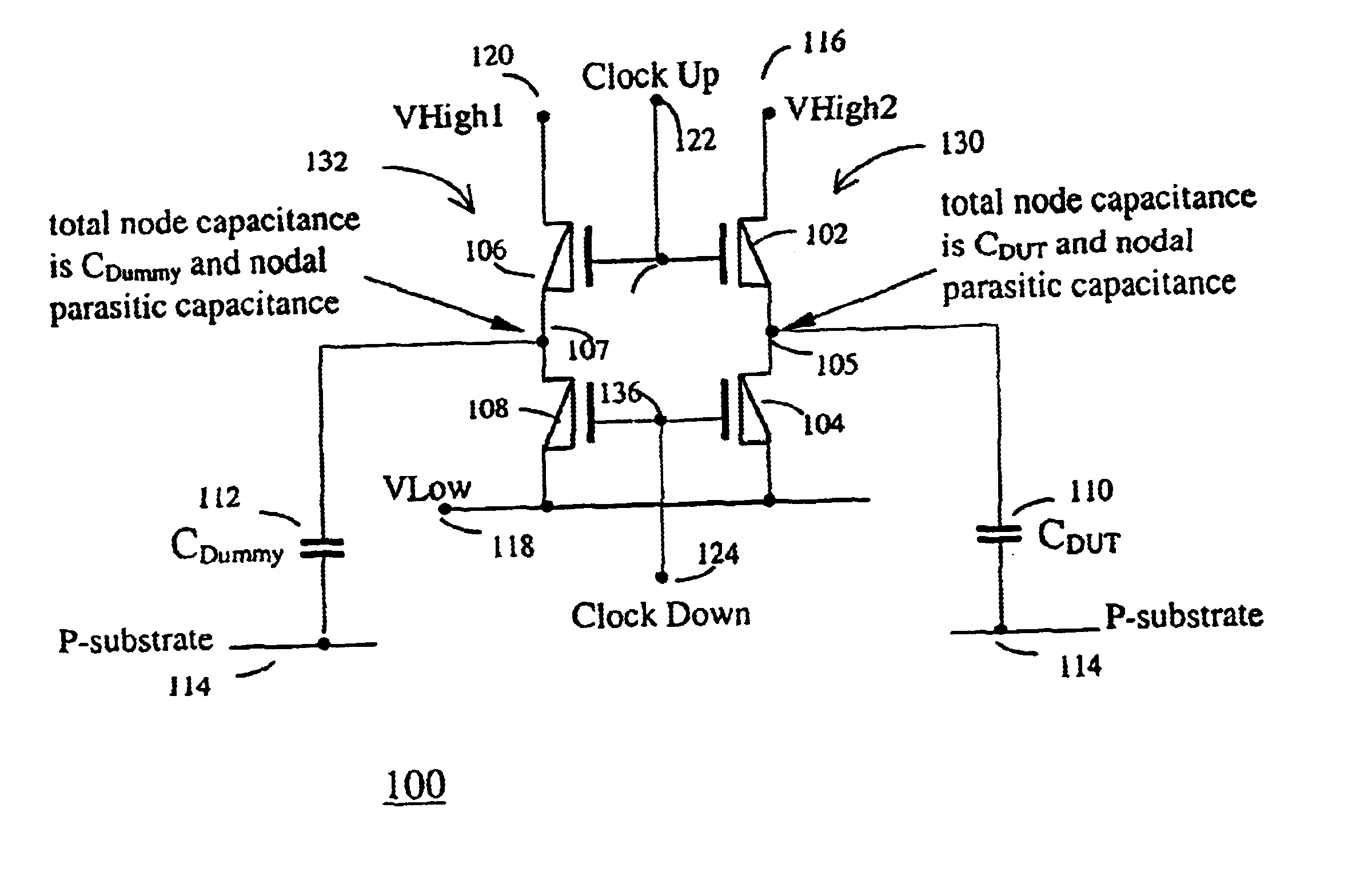
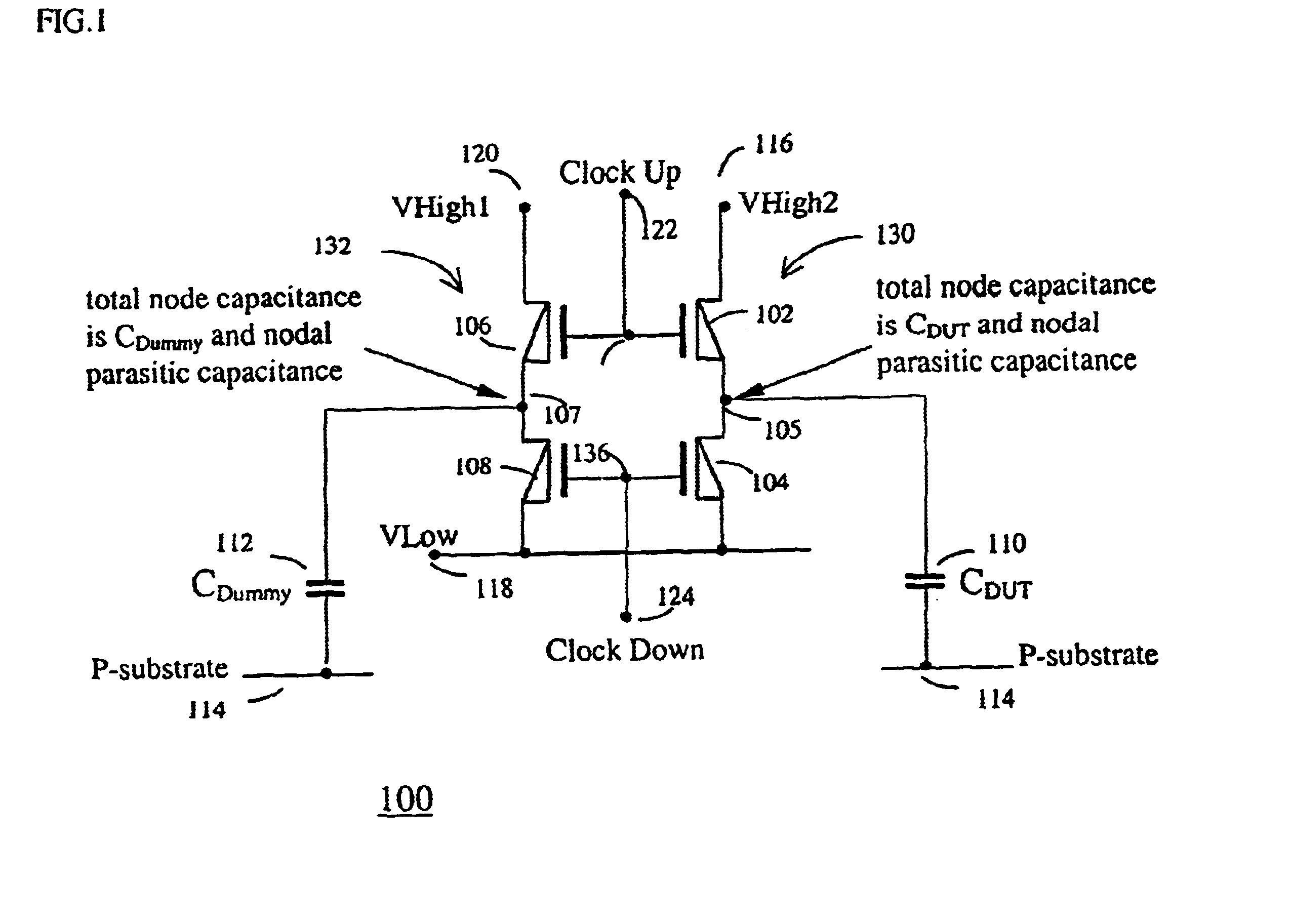
Referring now to FIG. 1, it shows a schematic diagram of a test circuit 100 used for measurement of integrated circuit parameters. The test circuit 100 includes a first transistor 102, a second transistor 104, a third transistor 106 and a fourth transistor 108. The third transistor is substantially the same in all regards as the first transistor. The fourth transistor is substantially the same in all regards to the second transistor. The test circuit 100 is connected to a device under test 110, in this case a capacitance labeled CDUT (Device Under Test Capacitance). In addition, the test circuit 100 includes a dummy capacitance 112, labeled CDUMMY. The device under test 110 is positioned between an output 105 of the test circuit 100 and the substrate 114. Similarly, the dummy capacitance 112 is electrically located between a node 107 and the substrate 114. Note that the device under test capacitance and the dummy capacitance are connected to the substrate 114 in this embodiment. Alt...


PUM


Abstract

A characterization method for a device under test includes applying a bias voltage to a test circuit. The test circuit includes a first transistor coupled to the device under test, a second transistor coupled to the device under test and to the first transistor. A third transistor is coupled to a dummy device, a fourth transistor is coupled to the dummy device and to the third transistor. The transistors are of a common type. The characterization method further includes applying non-overlapping clocking signals to transistors of the test circuit to produce test signals for application to the device under test and detecting a current in one or more transistors from the device under test. The bias voltage is further varied to characterize the device under test.

Description

BACKGROUNDThe present invention is related generally to test methods and structures for integrated circuits. In particular, the present invention is related to clocked based methods and devices for measuring voltage-variable capacitances and other on-chip parameters.Integrated circuits and their constituent components are tested for a variety of reasons. Completed circuits are tested for functionality and satisfaction of performance parameters. Such performance parameters include circuit speed or frequency of operation and power dissipation. Test cells on a circuit are tested for characterization of device parameters. Such device parameters include insulator dielectric capacitances, junction capacitances and threshold voltages in metal-oxide-semiconductor (MOS) integrated circuits, diode reverse bias leakage currents, dielectric tunneling currents, and, in non-volatile memory devices and standard MOS transistors, the location and density of trapped charges in gate dielectrics. Other...

Claims


Application Information

Patent Timeline
IPC IPC(8): G01R27/26G01R31/26H01L23/544
CPCG01R27/2605G01R31/2621H01L22/34H01L2924/0002H01L2924/00
Inventor ROGERS, DAVID MICHAELQIAN, MIMI XUEFENGTSAO, ROGER HUAZNEVAN BUSKIRK, MICHAEL ALLEN
Owner MONTEREY RES LLC
Why Eureka
Try Eureka