Optical profilometry of additional-material deviations in a periodic grating

a technology of additional materials and periodic gratings, which is applied in the direction of optical elements, instruments, chemical methods analysis, etc., can solve the problems of difficult formation of precise structures, limitations in current fabrication technologies, and constant pressure on the semiconductor microchip industry to reduce the dimensions of semiconductor devices

Inactive Publication Date: 2005-01-04
TOKYO ELECTRON US HOLDINGS INC
View PDF12 Cites 46 Cited by
  • Summary
  • Abstract
  • Description
  • Claims
  • Application Information

AI Technical Summary

Problems solved by technology

There is continual pressure on the semiconductor microchip industry to reduce the dimensions of semiconductor devices.
However, limitations in current fabrication technologies make formation of precise structures difficult.
For example, completely vertical sidewalls and completely horizontal top and bottom surfaces in device formation are difficult, if not impossible, to achieve.
While this is a non-destructive test, it does not provide profile information, but yields only a single number to characterize the quality of the fabrication process of the periodic structure.
Furthermore, the geometry of a structure in the periodic direction can also impact the geometry of successive layers of the chip.
While these techniques can generally adequately measure critical dimensions of structures having a single solid material along a line in the periodic direction, none of these techniques can make accurate measurements of critical dimensions of multiple material components of structures when more than a single solid material occurs in the periodic direction.
In particular, such techniques generally cannot make accurate measurements of materials having more than two materials in a periodic direction.
However, a process which is intended to produce a structure with only two materials per layer may have deviations which result in more than two materials in a layer.
And, as noted above, techniques discussed above which can measure critical dimensions of periodic structures having a nominal two materials in the periodic direction cannot be used to accurately measure the dimensions of multiple solid materials within structures having more than two materials in the periodic direction.
Specifically, techniques ordinarily used to measure the width of the ridges 815 will not yield an accurate measurement result when polymer 818 is present.
Accordingly, the idea of measuring the extent of any dishing occurring in a semiconductor manufacturing process has not generally arisen in the semiconductor fabrication industry since transverse deviations have not been considered to have substantial effects on the operation of devices or the fabrication of subsequent layers.

Method used


Image

  • Optical profilometry of additional-material deviations in a periodic grating
  • Optical profilometry of additional-material deviations in a periodic grating
  • Optical profilometry of additional-material deviations in a periodic grating

Examples


Embodiment Construction

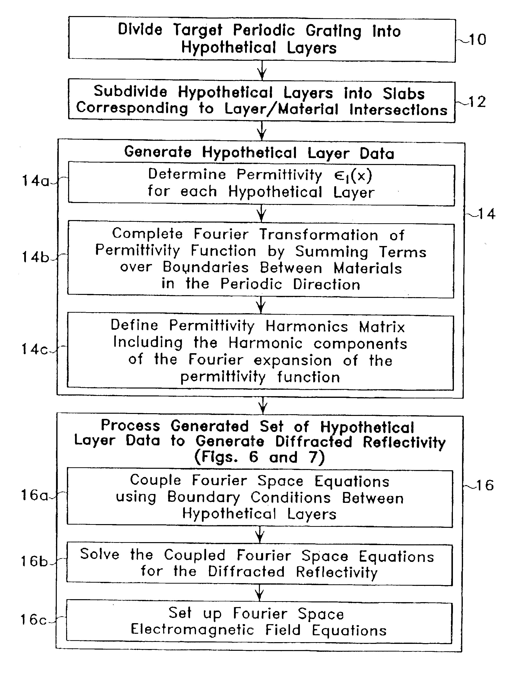
The present invention relates to metrology of additional-material deviations and deviations in a direction transverse to the critical dimension using a diffraction calculation technique. A system and method in accordance with the present invention can be used for the measurement of one-dimensionally periodic surface profiles, particularly where the surface profile has three or more materials along at least one line in the periodic direction.

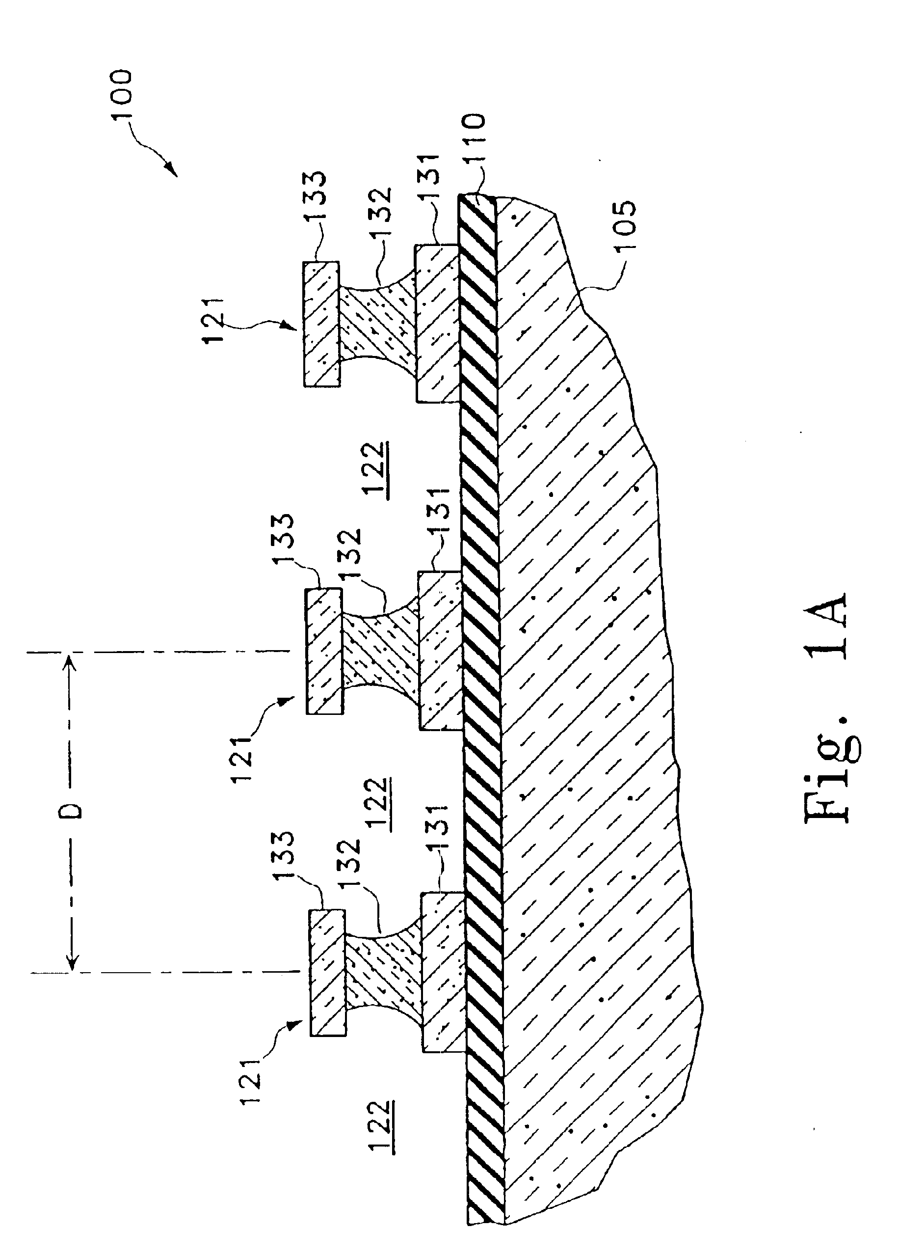
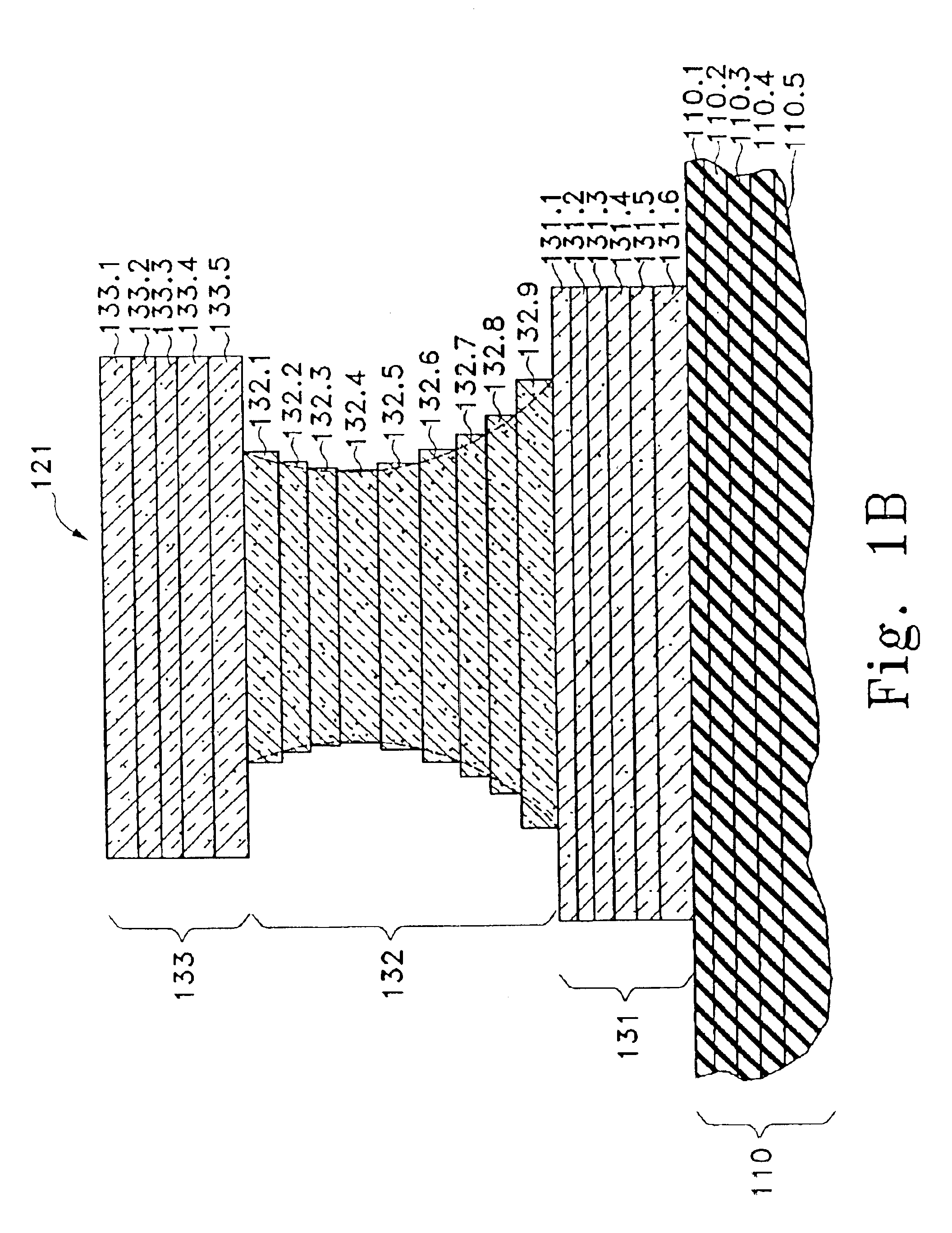
FIG. 4 is a diagram of a section of a periodic grating 600. The section of the grating 600 which is depicted includes three ridges 621 which are shown as having a triangular cross-section. It should be noted that the method of the present invention is applicable to cases where the ridges have shapes which are considerably more complex, and even to cases where the categories of “ridges” and “troughs” may be ill-defined. According to the lexography of the present specification, the term “ridge” will be used for one period of a periodic structure on...


PUM


Abstract

Disclosed is a method and system for measurement of periodic gratings which have deviations which result in more than two materials occurring along at least one line in the periodic direction. A periodic grating is divided into a plurality of hypothetical layers, each hypothetical layer having a normal vector orthogonal to the direction of periodicity, each hypothetical layer having a single material within any line parallel to the normal vector, and at least one of the hypothetical layers having at least three materials along a line in the direction of periodicity. A harmonic expansion of the permittivity ε or inverse permittivity 1 / ε is performed along the direction of periodicity for each of the layers including the layer which includes the first, second and third materials. Fourier space electromagnetic equations are then set up in each of the layers using the harmonic expansion of the permittivity E or inverse permittivity 1 / ε, and Fourier components of electric and magnetic fields in each layer. The Fourier space electromagnetic equations are then coupled based on boundary conditions between the layers, and solved to provide the calculated diffraction spectrum.

Description

TECHNICAL FIELDThe present invention relates generally to the measurement of periodic surface profiles using optical techniques such as spectroscopic ellipsometry. In particular, the present invention relates to optical profilometry of profile deviations of semiconductor fabrication processes, more particularly, additional-material deviations in a periodic grating.BACKGROUND OF THE INVENTIONThere is continual pressure on the semiconductor microchip industry to reduce the dimensions of semiconductor devices. Reduction in the size of semiconductor chips has been achieved by continually reducing the dimensions of transistors and other devices implemented on microchip arrays. As the scale of semiconductor devices decreases, control of the complete profile of the features is crucial for effective chip operation. However, limitations in current fabrication technologies make formation of precise structures difficult. For example, completely vertical sidewalls and completely horizontal top ...

Claims


Application Information

Patent Timeline
Patent Type & Authority Patents(United States)
IPC IPC(8): G02B27/42
CPCG01B11/0616G02B27/42G01B11/303G01B11/24
Inventor NIU, XINHUIJAKATDAR, NICKHIL
Owner TOKYO ELECTRON US HOLDINGS INC
Why Eureka
Try Eureka