Optical connection component

a technology of optical connection and component, applied in the direction of optics, optical waveguide light guide, instruments, etc., can solve the problems of loss of intactness of routing pattern, displacement of routing pattern, loss of protection layer, etc., and achieve the effect of high flexibility, easy handling, and high flexibility

Inactive Publication Date: 2005-01-04
TOMOEGAWA PAPER CO LTD +1
View PDF23 Cites 15 Cited by
  • Summary
  • Abstract
  • Description
  • Claims
  • Application Information

AI Technical Summary

Benefits of technology

The present invention has been completed with a view to resolving various problems of the conventional art such as those described above. Described specifically, an object of the present invention is to provide an optical interconnection apparatus free from attaching, fixing or adhering when came into contact with each other or with another material, and easy to handle. Another object of the present invention is to provide an optical interconnection apparatus having high flexibility and being easy to handle which makes it possible to readily interconnect optical components such as optical elements, optical circuit packs, optical circuit devices, etc.
A first aspect of the optical interconnection apparatus according to the present invention, which has a substrate, comprises a substrate, a protective resin layer composed of a silicone based rubber-like or gel-like material on one side or both sides of said substrate, and plural optical fibers which are two-dimensionally routed on the substrate so as to form a routing pattern having at least a crossing part, a curved part or a fiber pitch changing part and provided at ends thereof with end portions adapted to permit optical interconnections, and said optical fibers being held in place by said protective resin layer, wherein a non-tacky surface layer having a kinetic friction coefficient of 3 or less is provided on the surface of said protective resin layer. In an embodiment of the first aspect, it is possible to prepare an optical interconnection apparatus having plural substrates by laminating a protective resin layer formed on a substrate with another protective resin layer formed on another substrate via an adhesive layer.

Problems solved by technology

As these optical fibers have to be arranged with slacks in this case, it is a current practice that, on an optical circuit pack or inside and / or on a back side of an optical circuit devices, intricately routed lines of the optical fibers extend overlapping one another in the form of a bird's nest and hence occupy a large space.
This process is however accompanied by problems in that as optical fibers so located increase in number and the optical fibers increase more overlapped portions (cross-over routing) in the routing pattern so formed, the resulting routing layer of the optical fibers becomes thicker and, because the tacky surface with which the optical fibers are in contact becomes smaller at the overlapped portions of the optical fibers, the protective layer cannot be arranged evenly.
There is a further problem in that at the overlapped portions of the optical fibers in the routing pattern, the fixing force by the pressure-sensitive adhesive becomes weaker and the optical fibers are allowed to move, thereby resulting in displacements in the routing pattern (a loss in the intactness of the routing pattern).
The displacements in the routing patterns causes optical loss because of increased possibility of microbending of the optical fibers.
Furthermore, when the fixing force by the pressure-sensitive adhesive becomes weak, the optical circuit board becomes extremely weak to breakage which may be caused by deformation such as bending.
However, there is another problem that the silicone rubber-like or gel-like material causes attaching, fixing or adhering to the surface of, for example, metal, glass, high polymer (plastic), etc. by its characteristic of tackiness, whereby it becomes impossible to move in the optical interconnection apparatus.
Furthermore, there are problems because of its tackiness, that when plural optical interconnection apparatus are piled up upon storage, mounting or transportation, they adhere each other on their surfaces, thereby they being difficult to separate them, and that dust or other substance adheres on the surface of the optical circuit board, when it was installed in a rack or a board.
That is, when optical interconnection apparatus is installed in a very narrow space such as in a rack or a board, working efficiency became bad because of its tackiness to result in a problem of being hard to use.
Moreover, since the surface of the formed protective resin layer composed of a silicone based rubber-like or gel-like material is easily broken and damaged, there is a problem of surface scratches when the optical interconnection apparatus is installed in a very narrow space such as in a rack or a board.

Method used


Image

  • Optical connection component
  • Optical connection component
  • Optical connection component

Examples


first embodiment

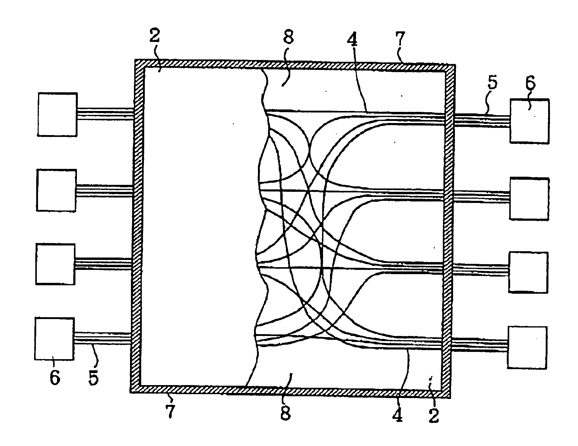
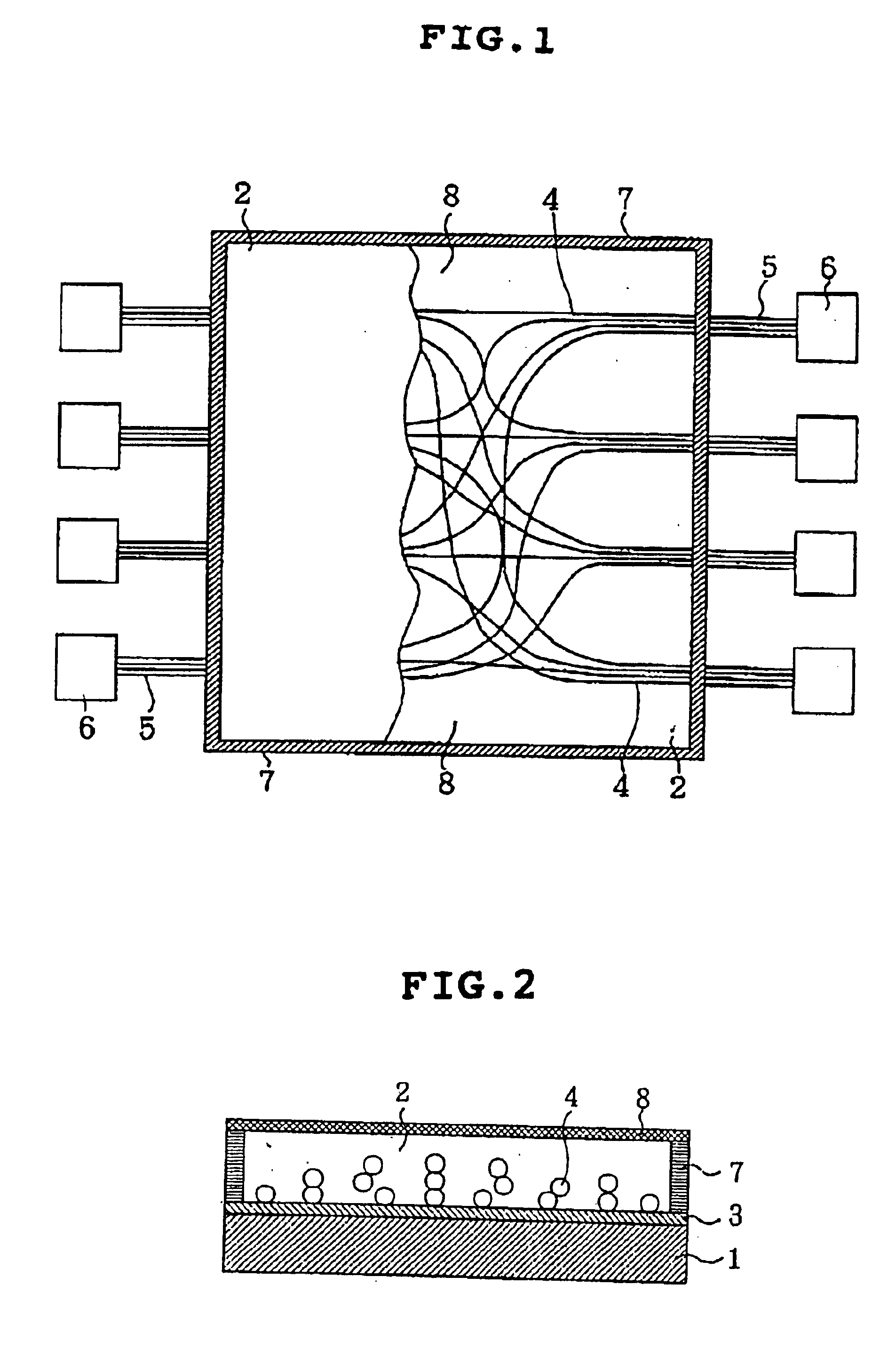
The optical interconnection apparatus of the first embodiment according to the present invention can be fabricated as will be described next. For example, an adhesive sheet is firstly produced by forming the above-mentioned adhesive layer on one side of a flexible film substrate having a two-dimensional plane. Optical fibers are then routed in a desired pattern by the above-described adhesive layer. At this time, the opposite ends of the optical fibers are located extending out from the film substrate such that they can be adapted as end portions for permitting optical interconnections with optical connectors or the like. As a process for arranging the adhesive layer, it is possible to adopt a process, in which the adhesive layer is arranged by coating an adhesive, either as it is or in the form of a coating material dissolved in a solvent, on the film substrate by a method such as roll coating, bar coating, blade coating, casting, dispenser coating, spray coating or screen coating,...

second embodiment

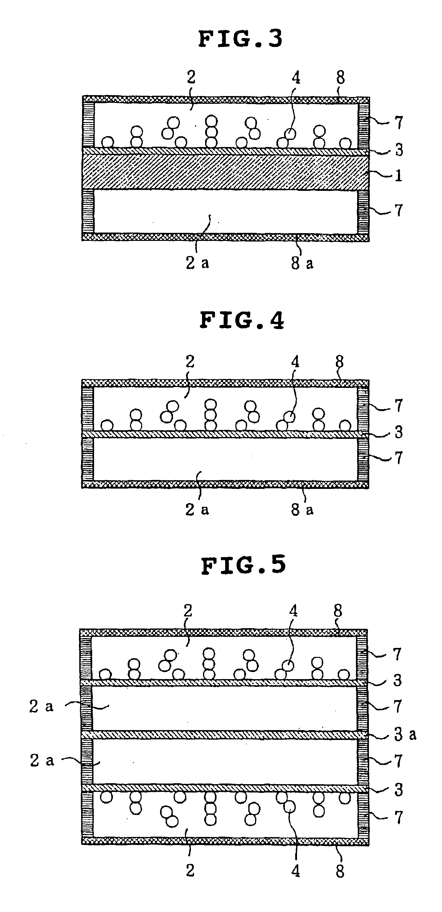
The optical interconnection apparatus of the second embodiment according to the present invention can be fabricated as will be described next. An adhesive sheet is first prepared by forming an adhesive layer on a release film, and optical fibers are routed in a desired pattern on the adhesive layer. Then, a protective resin layer is formed on the routed optical fibers. In concrete, the first protective resin layer is formed by arranging an edge-dam along or in the vicinity of the peripheral edges of the release film, and using a silicone-based rubber-like or gel-like material for producing an flexible protective resin layer. The release film on the back side is then removed. A second protective layer is thereafter formed on the exposed the first protective resin layer by arranging an edge-dam along or in the vicinity of the peripheral edges, and using a silicone-based material which is the same as or different from that of the first protective resin layer. On the resulted first and ...

example 1

An acrylic adhesive was applied to a side of a polyimide film of 125 μm in thickness so as to be a thickness of 100 μm to prepare a film substrate (size: 120 mm×100 mm). On the film substrate, optical fibers (product of The Furukawa Electric Co., Ltd., 250 μm in diameter) were routed per port (an exit of optical fibers from an optical interconnection apparatus) as follows. Namely, 4 optical fibers were arranged in parallel with each other at pitches of 250 μm per port, and 4 ports (each port was formed of 4 optical fibers) were formed at pitches of 30 mm on each of opposite sides, i.e., longer sides of the polyimide film. Each optical fiber was routed extending from one of the longer sides of the polyimide film to the other longer side. The routing to the individual ports on the opposite sides was designed such a manner that each of the optical fibers intersected in the central part of the sheet and the maximum overlapped number of optical fibers was 4 fibers.

Around the polyimide fi...


PUM


Abstract

The present invention provides an optical interconnection apparatus free from attaching, fixing or adhering when come into contact with each other or with another material, and easy to handle. The optical interconnection apparatus according to the invention comprises a substrate (1), a protective resin layer (2) composed of a silicone based rubber-like or gel-like material on one side or both sides of said substrate, and plural optical fibers (4) which are routed two-dimensionally routed on the substrate and provided at ends thereof with end portions (5) adapted to permit optical interconnections, and said optical fibers being held in place by said protective resin layer, wherein a non-tacky surface layer (8) is provided on the surface of said protective resin layer. The non-tacky surface layer is preferred to be composed of a silicone-based material and having a kinetic friction coefficient of 3.0 or less.

Description

TECHNICAL FIELDThis invention relates to optical interconnection apparatus (optical circuit board connectors) for mutually connecting optical component, parts and / or devices used in optical communications or optical information processing, such as optical elements, optical circuit packs and optical circuit devices.BACKGROUND ARTTo permit optical interconnections between plural optical components in an optical circuit pack or optical interconnections between plural optical circuit packs or between optical circuit devices on each of which optical circuit packs are mounted, these optical components, optical circuit packs and optical circuit devices are provided at terminals thereof with optical connectors to interconnect them together via optical fibers. As these optical fibers have to be arranged with slacks in this case, it is a current practice that, on an optical circuit pack or inside and / or on a back side of an optical circuit devices, intricately routed lines of the optical fibe...

Claims


Application Information

Patent Timeline
Patent Type & Authority Patents(United States)
IPC IPC(8): G02B6/36G02B6/43G02B6/38G02B6/42
CPCG02B6/3608G02B6/43G02B6/4239G02B6/3889G02B6/38875G02B6/00
Inventor KAWASE, RITSUSUKEGAWA, KENKOBAYASHI, TATSUSHIARISHIMA, KOICHIHIRAYAMA, MAMORU
Owner TOMOEGAWA PAPER CO LTD
Why Eureka
Try Eureka