Optical switching system based on hollow waveguides

a switching system and optical technology, applied in the field of optical switching system based on hollow waveguides, can solve the problems low insertion loss, and high insertion loss, and achieve the effect of low insertion loss

Inactive Publication Date: 2005-01-04
TERRAOP
View PDF4 Cites 19 Cited by
  • Summary
  • Abstract
  • Description
  • Claims
  • Application Information

AI Technical Summary

Benefits of technology

The present invention relates to integrated, chip based, fast optical switching systems, specifically optical switching systems incorporating hollow waveguides produced by MEMS technology, and operated digitally. Most specifically, the present invention discloses a novel, hollow waveguide based optical switch, and novel hollow waveguide-based switch architectures for optical communications. In con...

Problems solved by technology

Most of the currently available solutions have slow switching times, in the order of milliseconds, high insertion loss and lack scale-up capabilities.
On the other hand, there are a number of technologies that have high switching speed, but are fundamentally limited in the number of ports.
3-D MEMS devices involve a much more intricate design and driver set.
2-D MEMS components suffer from high insertion loss and cross talk, and cannot be easily scaled to a high port count as a result of the fact that the number of nodes of the crossbar equals the square of the port count number.
3-D MEMS components suffer from complex control system and high production cost, and therefore have low cost effectiveness.
Both technologies operate in the millisecond switching speed domain, and are therefore not suited for IP routing and other high speed switching applications.
Operational instabilities, high insertion loss and operational speed of milliseconds are the main drawbacks of this technology.
Limitations of liquid crystal technologies includ...

Method used


Image

  • Optical switching system based on hollow waveguides
  • Optical switching system based on hollow waveguides
  • Optical switching system based on hollow waveguides

Examples


Embodiment Construction

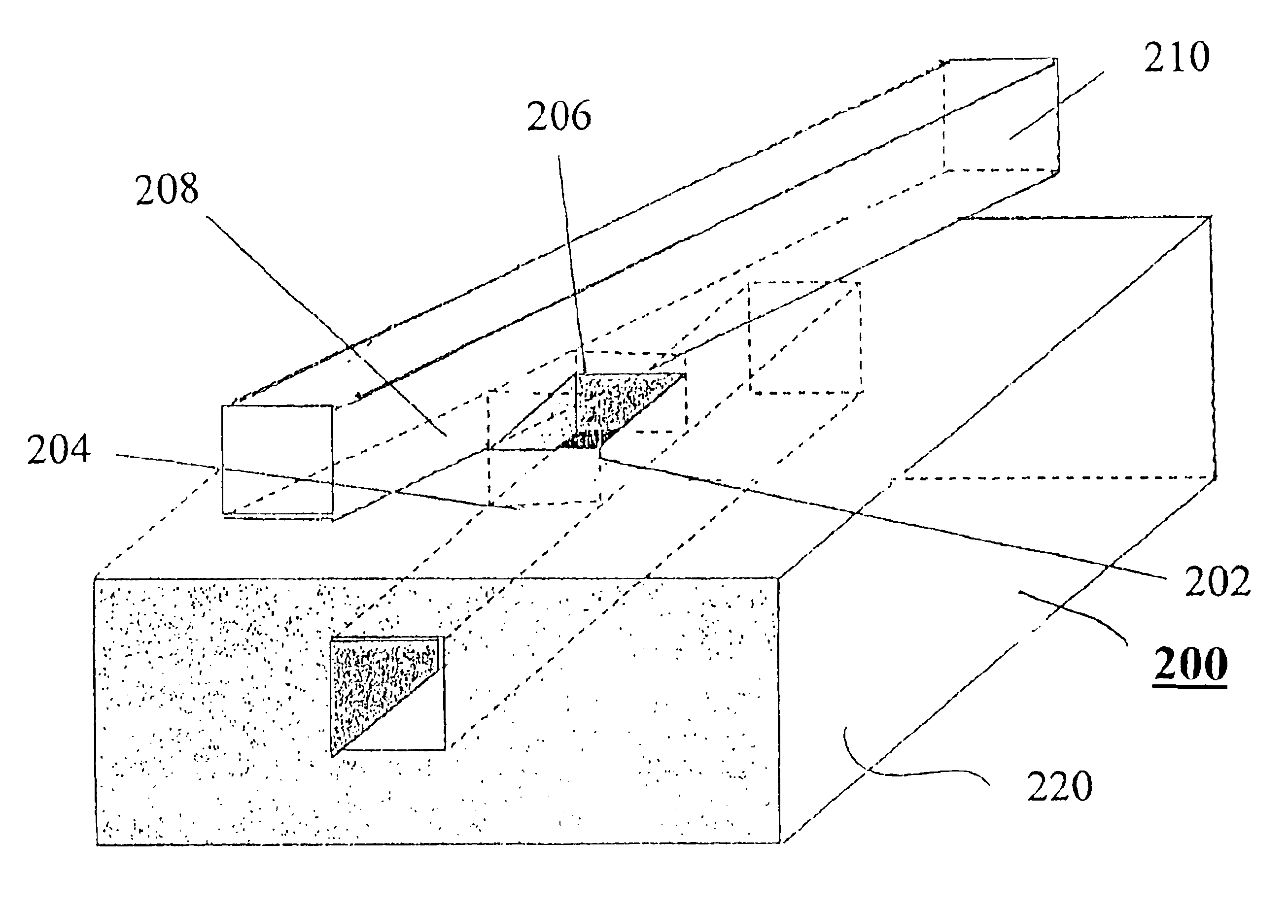
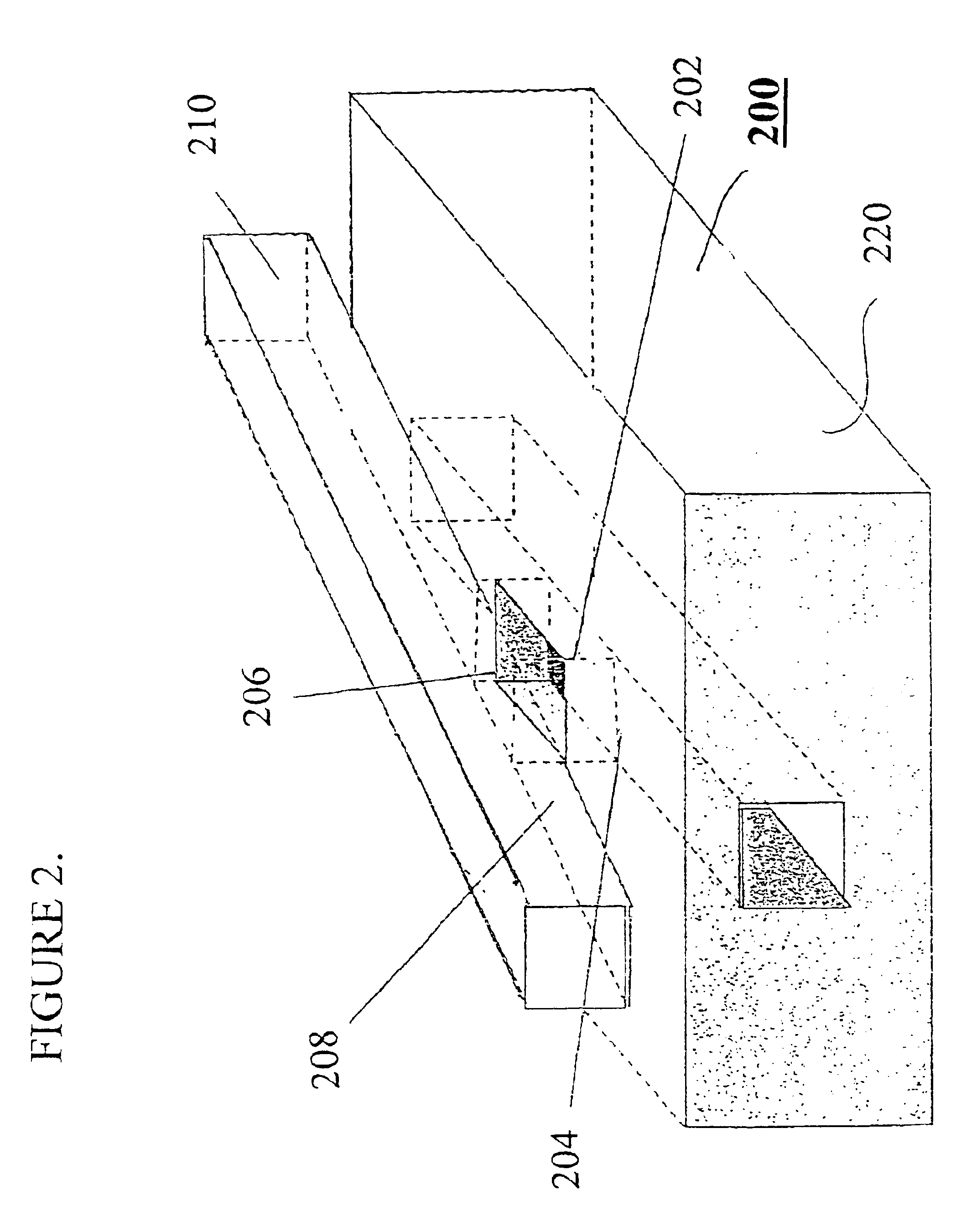
The present invention relates to integrated, chip-based, optical switching systems, specifically optical switching systems incorporating waveguides. More specifically, the present invention discloses an optical switching system based on hollow waveguides. The principles and operation of an optical switching system based on hollow waveguides according to the present invention may be better understood with reference to the drawings and the accompanying description. As mentioned above, various HW structures, as well as fabrication processes are known in the art. The invention described herein may be implemented using such known waveguides and fabrication processes.

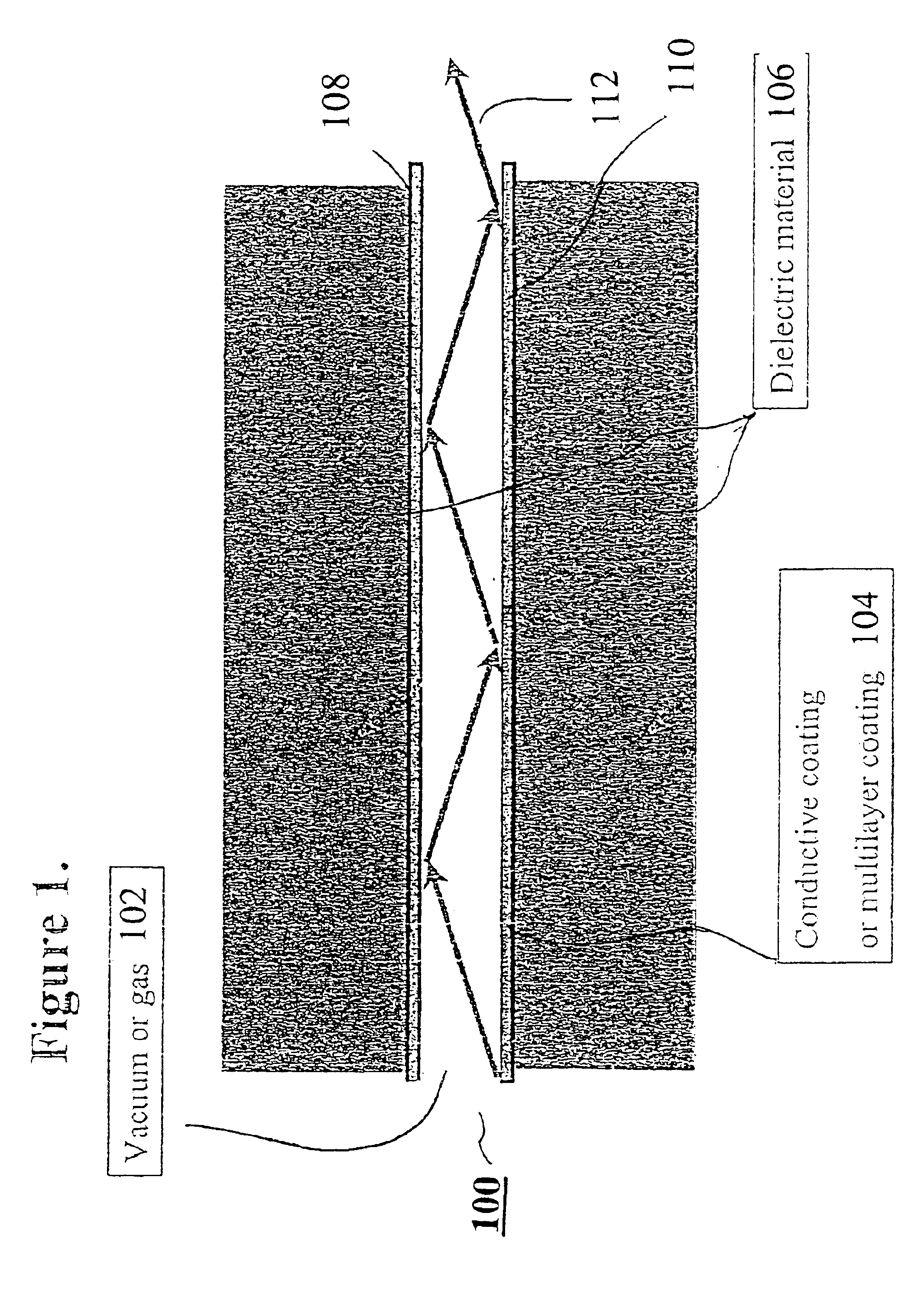
FIG. 1 shows a longitudinal cross section of a HW 100 that includes a hollow (vacuum or gas filled) core 102 that can have a cross section of any shape (rectangular, round, hexagonal, etc.). The core is surrounded by a reflective coating 104 that may be single layered or multilayered, conductive or dielectric, and by an addit...


PUM


Abstract

A hollow waveguide based optical switch, and novel hollow waveguide-based switch architectures for optical communications. The switch comprises a pair of hollow waveguides overlapping over a common section that includes a common opening, a first conductive flexible lever attached to one of the hollow waveguides, the first lever configured to assume upon actuation at least two switching positions within the pair of waveguides at the common opening, a second conductive flexible lever attached to the other of the hollow waveguides, the second lever configured to assume upon same the actuation same at least two switching positions within the pair of waveguides as the first lever while keeping a substantially parallel geometry with the first lever, and means to actuate the first and the second levers in order to achieve the at least two switching positions.

Description

FIELD AND BACKGROUND OF THE INVENTIONGrowing demand for bandwidth is fueling the need for advances in optically based telecommunications. Many of these advances are provided by new developments in optical components. Most of the currently available solutions have slow switching times, in the order of milliseconds, high insertion loss and lack scale-up capabilities. On the other hand, there are a number of technologies that have high switching speed, but are fundamentally limited in the number of ports. Following is a short review of existing optical component technologies for both active (e.g. switching) and passive (e.g. splitting) applications.MEMS (Micro Electro Mechanical Systems) technology is a relatively mature and cost effective technology, in use for more than 10 years for commercial applications. There are two primary types of MEMS optical components or devices: 2-D (2 dimensional architecture) and 3-D (3 dimensional architecture) devices. 2-D or digital MEMS devices opera...

Claims


Application Information

Patent Timeline
IPC IPC(8): G02B6/125G02B6/122G02B6/35G02B6/12
CPCG02B6/122G02B6/125G02B6/3502G02B6/3536G02B6/032G02B2006/12145G02B6/3556G02B6/357G02B6/3584G02B2006/12119
Inventor HUBER, TALYAHUBER, AVIGDOR
Owner TERRAOP
Why Eureka
Try Eureka