Wiring substrate
- Summary
- Abstract
- Description
- Claims
- Application Information
AI Technical Summary
Benefits of technology
Problems solved by technology
Method used
Image
Examples
second embodiment
Next, a wiring substrate of the invention will be described.
In this embodiment, the components corresponding to those in the structure of the first embodiment bear the same reference numeral, and the description thereof will be omitted.
In this embodiment, the structure of the wiring substrate is similar to that of the first embodiment, and the aspect to be noted is that the electroless plated metal layer contains a platinum group metal and is free from lead.
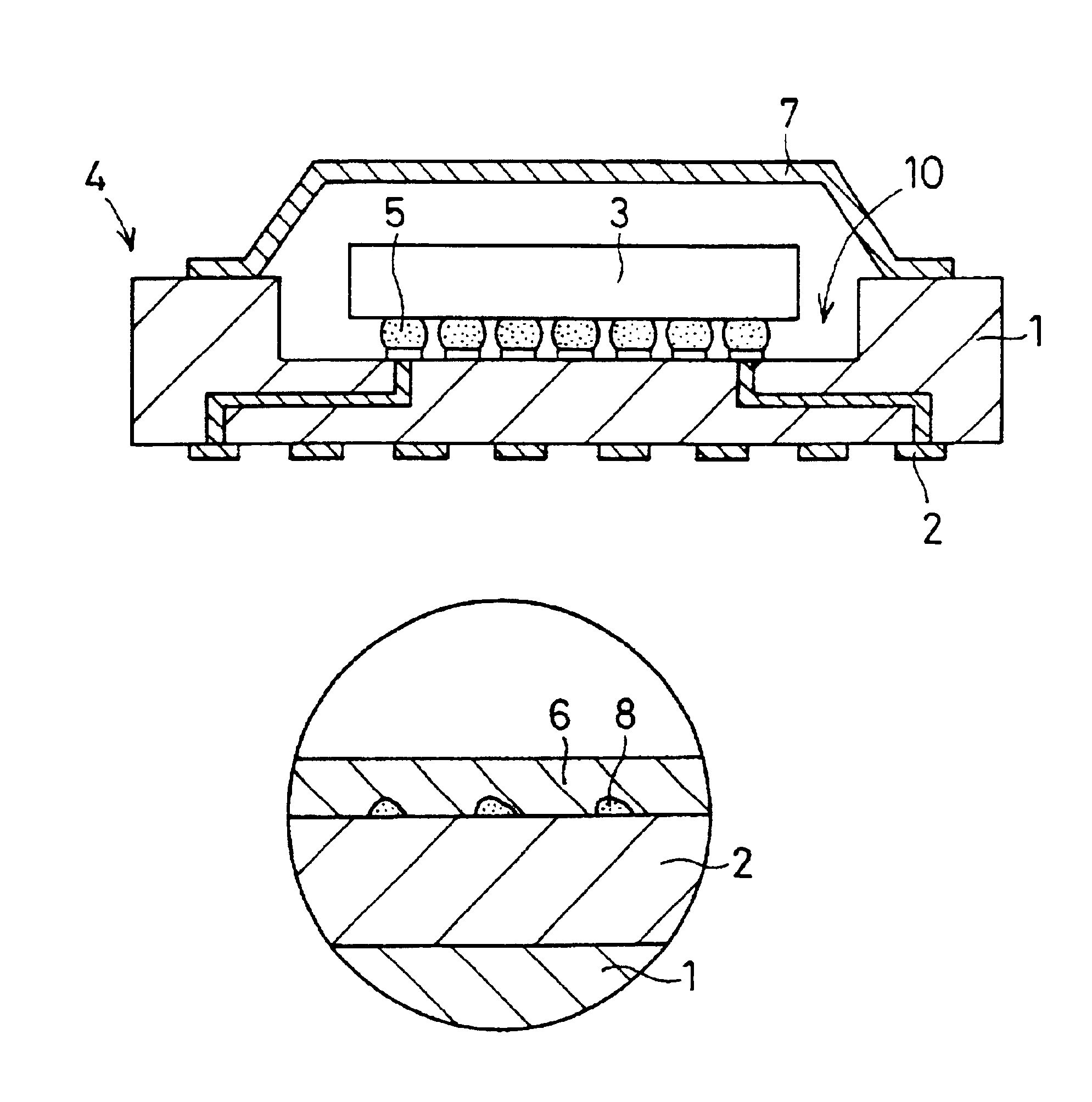
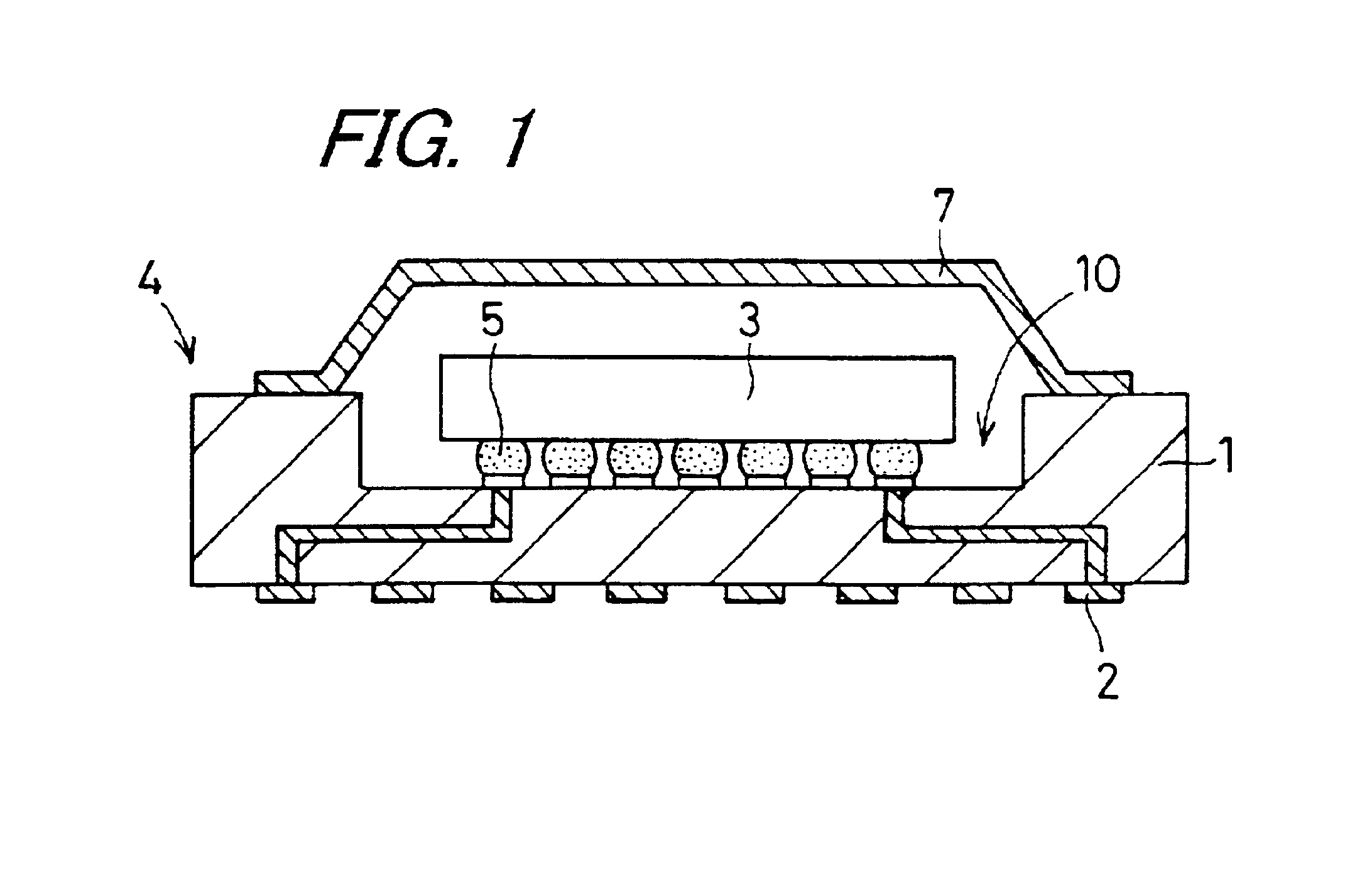
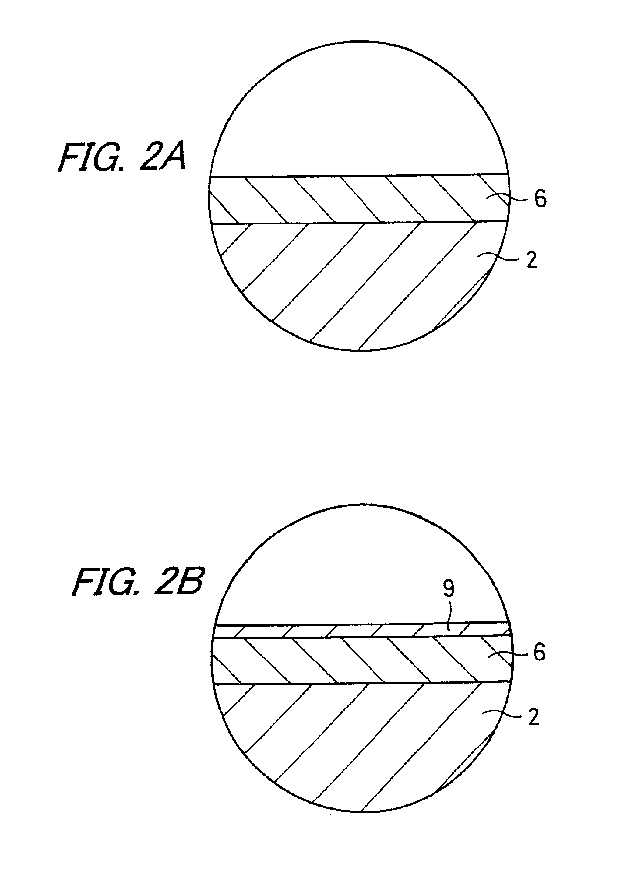
FIG. 4A is an enlarged sectional view showing an enlarged part of the wiring substrate of the second embodiment of the invention. The surface of the wiring conductor 2 is coated with the plated metal layer 16 by electroless plating, as shown in the sectional view of FIG. 4A. The plated metal layer 16 serves to improve the wettability, the joining strength, and the bonding properties of solders with respect to the wiring conductor 2 and is made of a high purity nickel that contains nickel in a content of 99.9 wt %, a nickel-phosph...
PUM
| Property | Measurement | Unit |
|---|---|---|
| Digital information | aaaaa | aaaaa |
| Melting point | aaaaa | aaaaa |
Abstract
Description
Claims
Application Information


