Electrical circuit apparatus and method for assembling same

a technology of electrical circuit apparatus and assembly method, which is applied in the direction of printed circuit non-printed electric component association, metal adhesion improvement of insulating substrate, and electric connection formation of printed elements. it can solve the problems of affecting the effect of the ground attachment, and requiring manual processing

Inactive Publication Date: 2005-01-11
MOTOROLA SOLUTIONS INC
View PDF10 Cites 34 Cited by
  • Summary
  • Abstract
  • Description
  • Claims
  • Application Information

AI Technical Summary

Benefits of technology

A number of exemplary advantages over the prior art can be realized using the method and electrical circuit apparatus of the present invention, wherein power devices may be mounted to a circuit board. These advantages include, but are not limited to: (1) repeatable solder attachment of a power device in two planes or regions (i.e., at the input and output terminals and at the ground flange); (2) a good thermal path from the bottom of the power device, though its ground flange, to a heat sink directly below; (3) repeatable solder attachment of the ground layer of the circuit board to the heat sink, the solder attachment being under the input and output terminals and as close as possible to the body of the power device; (4) mechanical attachment of the heat sink to the circuit board to add robustness to assembly for handling and subsequent module assembly; (5) elimination of the need for fixtures in a one-step or single pass reflow soldering process that lends itself to no-lead solder or leaded solder; and (6) assembly can be accomplished during SMT attachment of other components to the circuit board without requiring additional process steps.

Problems solved by technology

Due to the fragility of the substrate, large fixtures are usually required for its alignment and protection during processing.
The use of fixtures usually forces manual processing.
One disadvantage of the hybrid manufacturing process is that it is more costly than other manufacturing methods primarily due to the added cost of the fixtures used in the process and also due to the need for a number of manual steps that generate a lower production throughput.
An additional disadvantage is that manufacturing with fixtures produces a significant variation in the ground attachment relative to the signal lines to which the transistor terminals are attached.
A primary disadvantage of the two pass reflow process is that it requires one high-temperature reflow pass with a high melting temperature solder alloy, and a second subsequent reflow pass with a lower melting temperature solder allow.
The first pass exposes the circuit board to high temperature, which can result in damage such as distortion.
The requirement of two independent passes with different solder temperature settings limits manufacturing throughput.
The two pass approach also does not lend itself well to no-lead solder because the first temperature needed to attach the heat sinks would have to exceed the elevated no-lead solder reflow temperature.
This is a significant disadvantage because no-lead solder attachment may likely become a key product differentiator in the near future since some markets, especially European markets, are moving toward requiring no-lead solder attachment.

Method used


Image

  • Electrical circuit apparatus and method for assembling same
  • Electrical circuit apparatus and method for assembling same
  • Electrical circuit apparatus and method for assembling same

Examples


Embodiment Construction

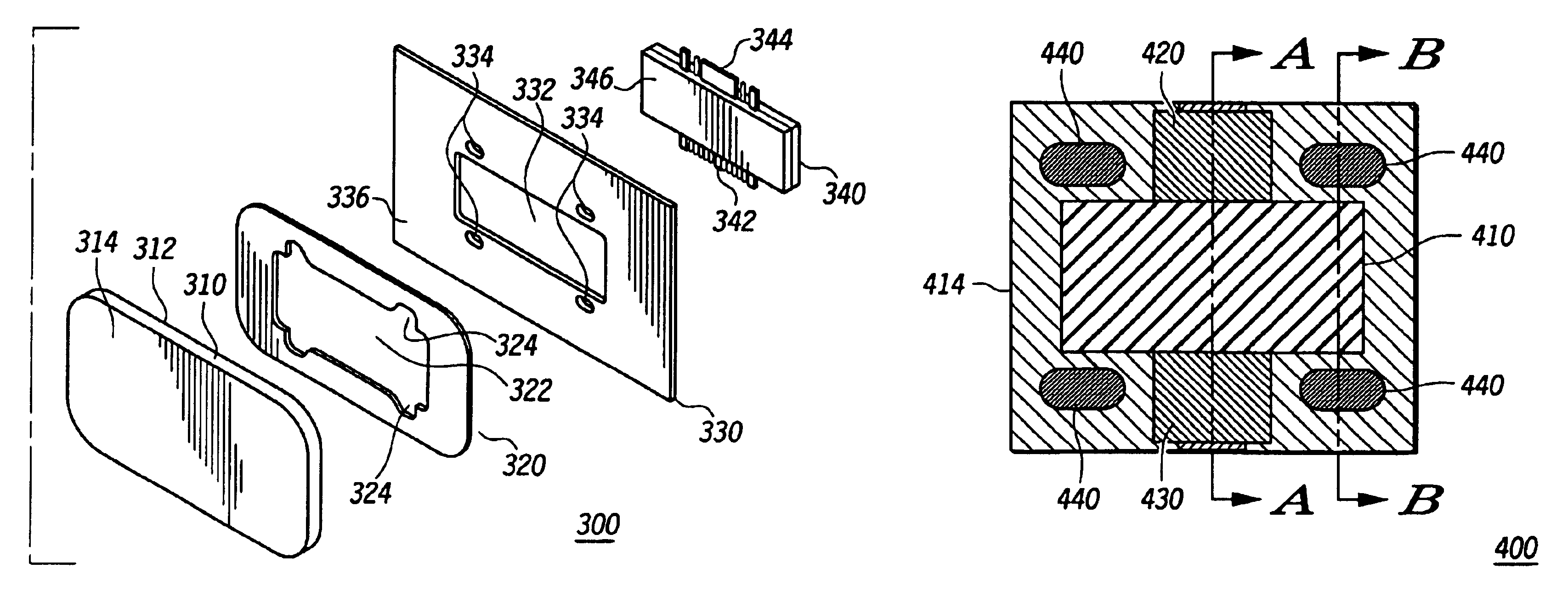
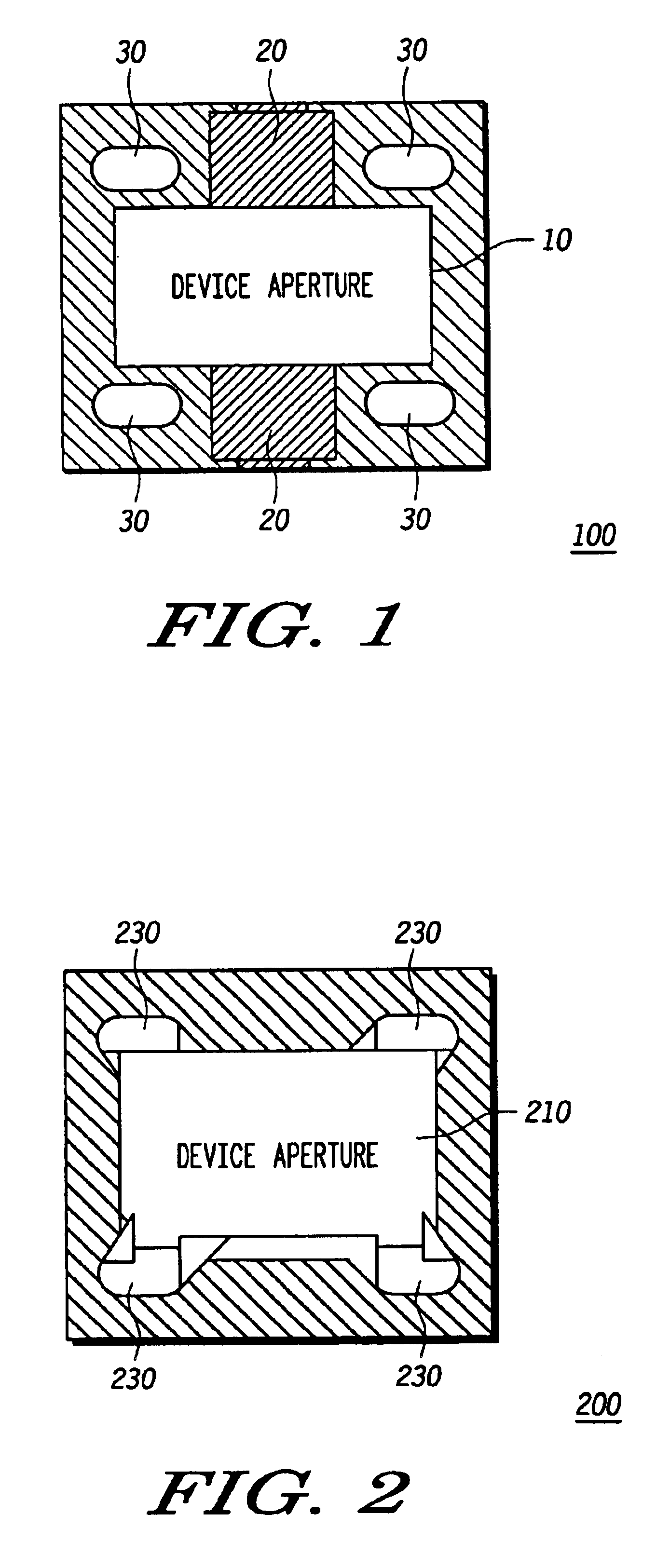
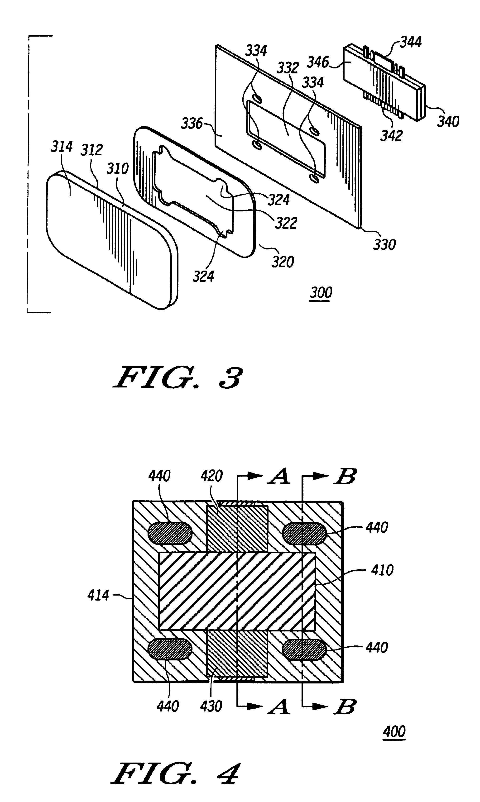
While this invention is susceptible of embodiments in many different forms, there are shown in the figures and will herein be described in detail specific embodiments, with the understanding that the present disclosure is to be considered as an example of the principles of the invention and not intended to limit the invention to the specific embodiments shown and described. Further, the terms and words used herein are not to be considered limiting, but rather merely descriptive. It will also be appreciated that for simplicity and clarity of illustration, elements shown in the figures have not necessarily been drawn to scale. For example, the dimensions of some of the elements are exaggerated relative to each other. Further, where considered appropriate, reference numerals have been repeated among the figures to indicate corresponding elements.

The present invention includes a method and electrical circuit apparatus, wherein components, namely power devices including RF transistors, m...


PUM


Abstract

An electrical circuit apparatus (300) that includes: a substrate (330) having a ground layer (336), at least one device aperture (332), and at least one solder aperture (334); a heat sink (310); and an adhesive layer (320) for mechanically coupling the heat sink to the ground layer of the substrate such that at least a portion of the substrate device aperture overlaps the heat sink, the adhesive layer having at least one device aperture and at least one solder aperture, wherein aligning the at least one substrate solder aperture with the at least one adhesive layer solder aperture and aligning the at least one substrate device aperture with the at least one adhesive layer device aperture enables solder wetting in a predetermined area between the heat sink and the ground layer of the substrate.

Description

FIELD OF THE INVENTIONThe present invention relates generally to mounting a component to a circuit board, and more specifically to mounting a power device, such as a radio frequency (“RF”) transistor to a circuit board.BACKGROUND OF THE INVENTIONWhen constructing power amplifiers various components must be mounted to a circuit board or substrate. One such component is a power component or power device such as, for instance, a power transistor, also referred to herein as a radio frequency (or “RF”) transistor. When mounting an RF transistor that includes one or more input terminals and one or more output terminals to a circuit board with corresponding input and output signal lines, two factors must be balanced, i.e., the need for a proper electrical coupling of the device to the circuit board must be balanced against the high heat dissipation needs of the device. To provide for optimal electrical performance of the power transistor both the input and the output terminals are typicall...

Claims


Application Information

Patent Timeline
Patent Type & Authority Patents(United States)
IPC IPC(8): H05K1/02H05K3/00H05K3/40H05K3/34H05K3/38H05K1/18
CPCH05K1/021H05K1/182H05K3/0061H05K3/341H05K3/386H05K2203/063H05K2201/0305H05K2201/09554H05K2201/10166H05K2201/10969H05K2203/042H05K3/4038
Inventor WALDVOGEL, JOHN M.BIELICK, BRIAN R.MILLER, HERMAN J.VAN CANNON, BILLY J.
Owner MOTOROLA SOLUTIONS INC
Why Eureka
Try Eureka