III-nitride light-emitting device with increased light generating capability

Inactive Publication Date: 2005-01-18
LUMILEDS +1
View PDF64 Cites 78 Cited by
  • Summary
  • Abstract
  • Description
  • Claims
  • Application Information

AI Technical Summary

Benefits of technology

The present invention is an inverted III-nitride light-emitting device (LED) with enhanced total light generating capability. A large area (>400×400 μm2) device has at least one n-electrode which interposes the p-electrode metallization to provide low series resistance. The p-electrode metallization is opaque, highly reflective, Ohmic (specific contact resistance less than 10−2 Ωcm2), and provides excellent current spreading. Light absorption in the p-electrode at the peak emission wavelength of the LED active region is less than 25% per pass. An intermediate material or submount may be used

Problems solved by technology

There are some unique challenges in the fabrication of III-nitride semiconductor devices.
Because III-nitride substrates are not commercially available, the epitaxial growth is forced to occur upon non-lattice-matched substrates, e.g. sapphire or SiC.
However, even these thin semi-transparent layers absorb a significant amount of light.
Increasing the metal thickness increases light absorption and reduces the extraction efficiency of the device.
Light extraction efficiency is limited by the amount of surface area covered by this Ohmic electrode and by the bonding pads.
Since this device lacks a highly reflective p-electrode metallization, it is limited in terms of light extraction efficiency and does not offer a significant improvement over the conventional (epitaxy-side up) device.
Also, because the devices are small (<400×400 μm2) and use a small solder connection area to the package, they are limited in their light generating capability.
Finally, this device suffers in efficiency from having guided light trapped within the III-nitride epi layers because of the low-refractive-index sapphire superstrate.
However, Ag adhesion to III-nitride material is poor.
Upon annealing, Ag can conglomerate and destroy the integrity of the sheet Ohmic contact behavior and the reflectivity.
Since the devi

Method used


Image

  • III-nitride light-emitting device with increased light generating capability
  • III-nitride light-emitting device with increased light generating capability
  • III-nitride light-emitting device with increased light generating capability

Examples


Example

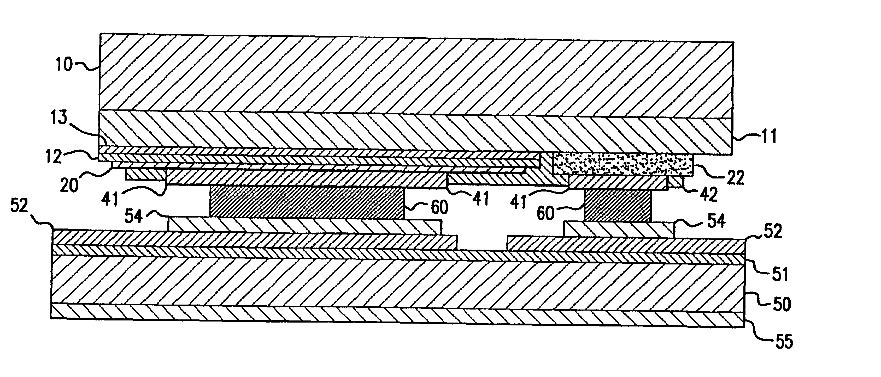
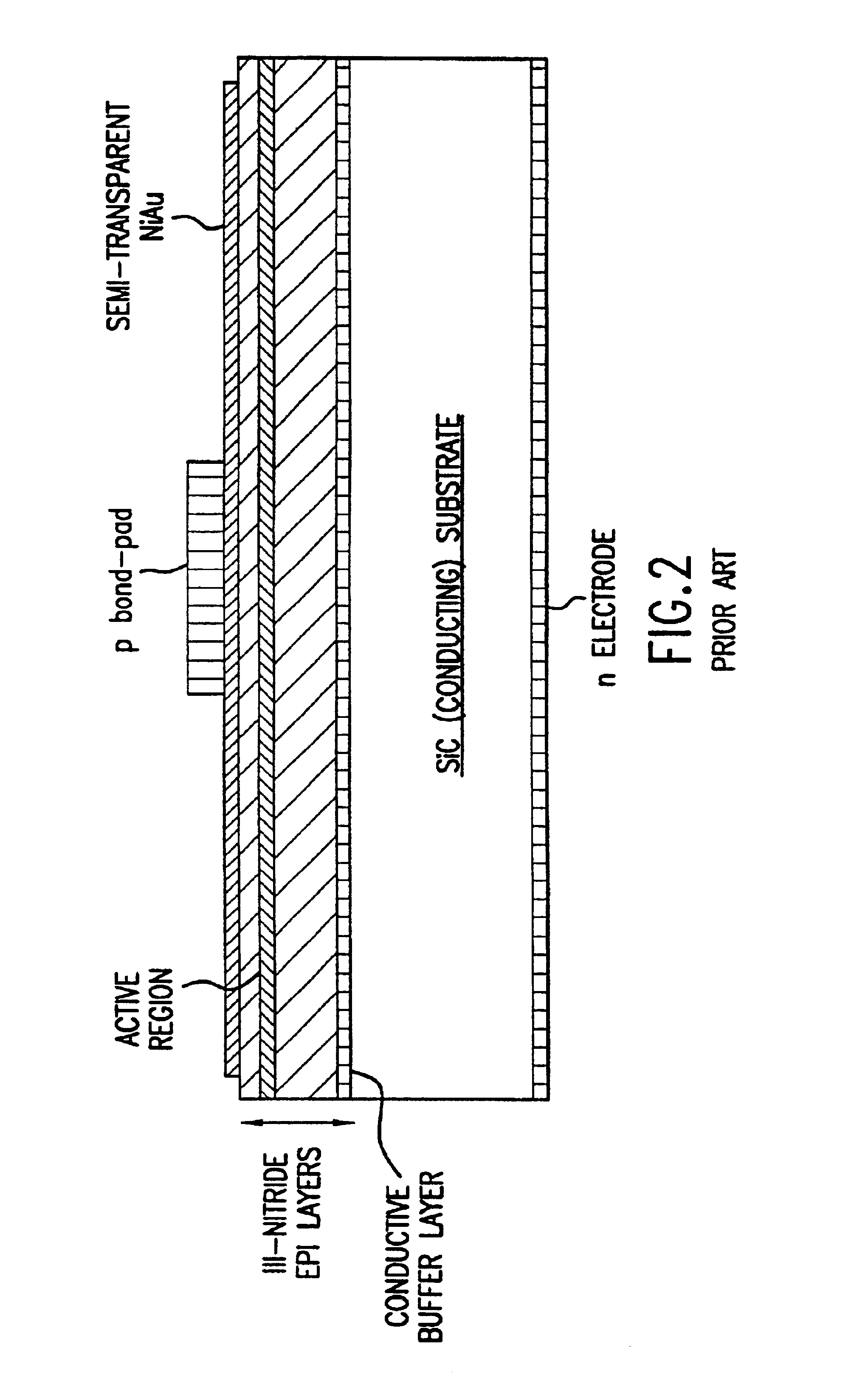
One fundamental limiting condition of LED operation is maximum junction temperature. The maximum junction temperature, Tjmax, is the temperature of the p-n junction region at which breakdown or failure occurs in some part of the LED or its housing. This breakdown often occurs as the glass transition temperature of an encapsulating epoxy or lens is approached, causing loss of transparency and eventual melting of these materials. With such a limit established, ΔTj, the temperature rise from ambient to Tjmax, may be expressed as (assuming power conversion efficiency<<100% which is true for present-day III-nitride devices),

ΔTj=Tjmax−Ta=ImaxVfΦj-a,  (1)

where Ta is the ambient temperature, Imax is the maximum operating current, and Vf is the forward voltage at that current, and Φj-a is the thermal resistance from the p-n junction to ambient. Inserting a simplified expression for Vf, and re-writing yields

Imax=ΔTj / [Φj-a(V0+ImaxRs)],  (2)

where V0 is the turn-on voltage (approxima...


PUM


Abstract

The present invention is an inverted III-nitride light-emitting device (LED) with enhanced total light generating capability. A large area device has an n-electrode that interposes the p-electrode metallization to provide low series resistance. The p-electrode metallization is opaque, highly reflective, and provides excellent current spreading. The p-electrode at the peak emission wavelength of the LED active region absorbs less than 25% of incident light per pass. A submount may be used to provide electrical and thermal connection between the LED die and the package. The submount material may be Si to provide electronic functionality such as voltage-compliance limiting operation. The entire device, including the LED-submount interface, is designed for low thermal resistance to allow for high current density operation. Finally, the device may include a high-refractive-index (n>1.8) superstrate.

Description

FIELD OF THE INVENTIONThe present invention relates to semiconductor light emitting devices, and more particularly to III-nitride based light-emitting devices with improved light generating capability.BACKGROUND OF THE INVENTIONA “III-nitride” material system is any combination of group III and group V elements, with nitrogen being the primary group V element, to form semiconductors used in the fabrication of electronic or optoelectronic devices. This material system includes, but is not limited to, GaN, AlGaN, AlN, GaInN, AlGaInN, InN, GaInAsN, and GaInPN. The III-nitride material system is suitable for the fabrication of light-emitting devices (LEDs) that generate light with photon energies from the ultra-violet to the red spectral wavelength regimes. These LEDs include light-emitting diodes and laser diodes.A III-nitride LED typically includes epitaxial layers deposited upon a suitable growth substrate to form a p-n junction via growth techniques, e.g. organometallic vapor-phase ...

Claims


Application Information

Patent Timeline
IPC IPC(8): H01L33/00H01L27/15H01L33/02H01L33/38H01L33/40H01L33/62H01L33/64
CPCH01L33/025H01L33/405G09G2360/148H01L27/156H01L33/20H01L33/38H01L2924/0002H01L33/62H01L33/641H01L33/647H01L2924/00H01L24/05H01L24/06H01L25/167H01L2224/05001H01L2224/05023H01L2224/05568H01L2224/05572H01L2224/06051H01L2224/14
Inventor KRAMES, MICHAEL RSTEIGERWALD, DANIEL A.KISH, JR., FRED A.RAJKOMAR, PRADEEPWIERER, JR., JONATHAN J.TAN, TUN S
Owner LUMILEDS
Why Eureka
Try Eureka