Integrated circuit test probe

a test probe and integrated circuit technology, applied in the field of test probes, can solve the problems of low conductivity of the junction, difficult assembly, and designed for high frequency applications, and achieve the effects of low insertion force parameter, extended life of test probes, and high electrical connectivity

Inactive Publication Date: 2005-01-18
ARIES ELECTRONICS
View PDF20 Cites 45 Cited by
  • Summary
  • Abstract
  • Description
  • Claims
  • Application Information

AI Technical Summary

Benefits of technology

The subject invention provides for a new and improved test probe for connecting an IC chip to a printed circuit board. The subject invention further provides for a new and improved test probe that is small enough to be used in the densities required by state of the art integrated circuit chips. In operation, the test probe of the subject invention maintains high electrical connectivity, while maintaining a low insertion force parameter so as to extend the life of the test probe and minimize damage to the leads of the IC chips under test.

Problems solved by technology

However, the device of Richards et al. is designed to score the connection surface of one device and is not designed for high frequency applications.
Scoring the surface of a component to remove the insulating coating is not desirable since it permits contaminants to contact the component's surface causing oxidation of the surface that results in lower conductivity of the junction.
The Reuter, et al. spring contact probe has, as described above, numerous components, is difficult to assemble, and is costly.
In addition, because of the many components, the electrical path during a testing operation is quite circuitous, thereby limiting the high frequency testing application of the Reuter, et al. probe.
Because of the construction of the Murphy socket terminal, the electrical path between the printed circuit board and the BGA component is also circuitous, and the numerous components result in an expensive socket terminal.
Furthermore, for RF applications, the circuitous electrical path results in high resistance, thereby limiting the application of the socket terminal.

Method used


Image

  • Integrated circuit test probe
  • Integrated circuit test probe
  • Integrated circuit test probe

Examples


Embodiment Construction

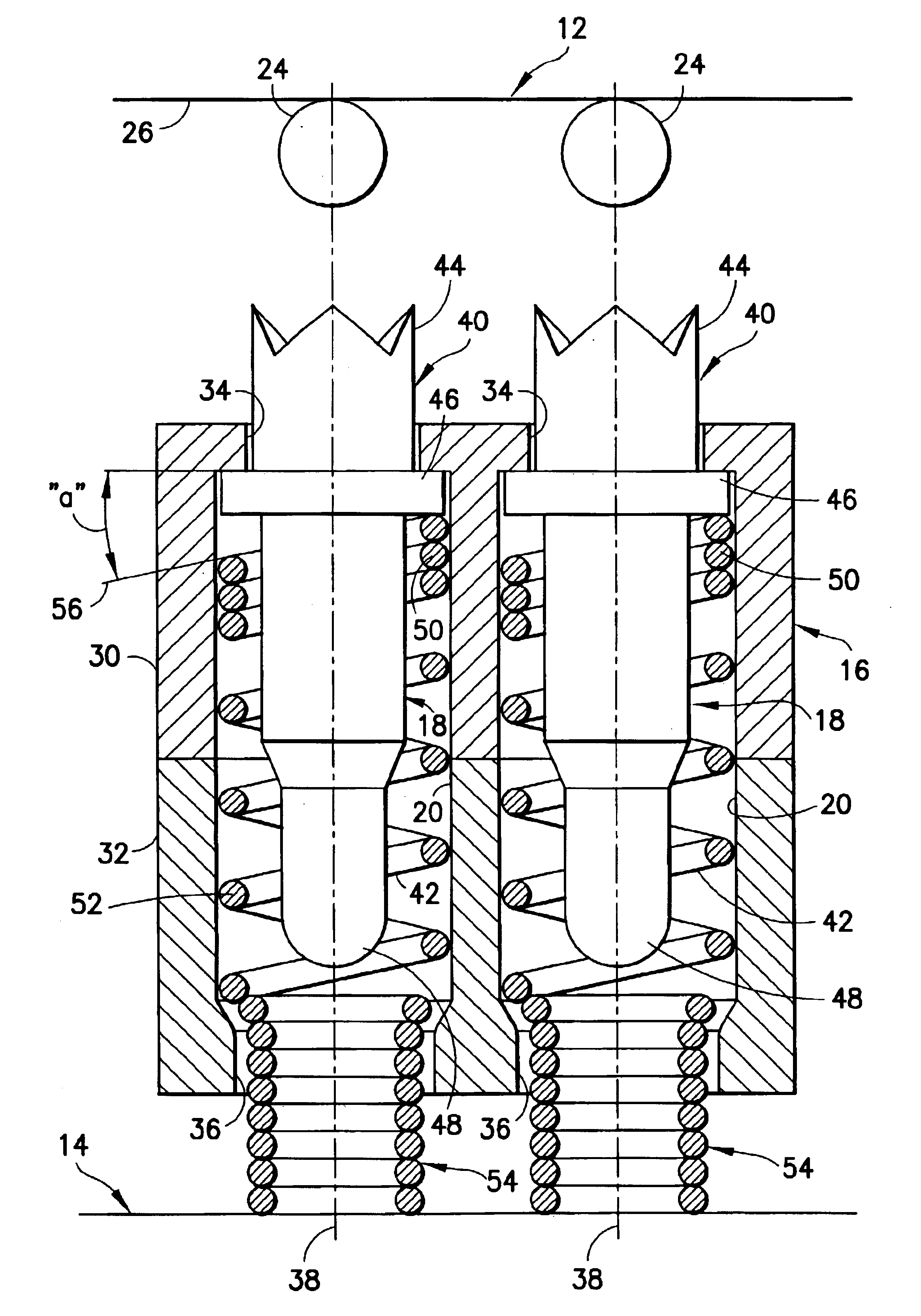
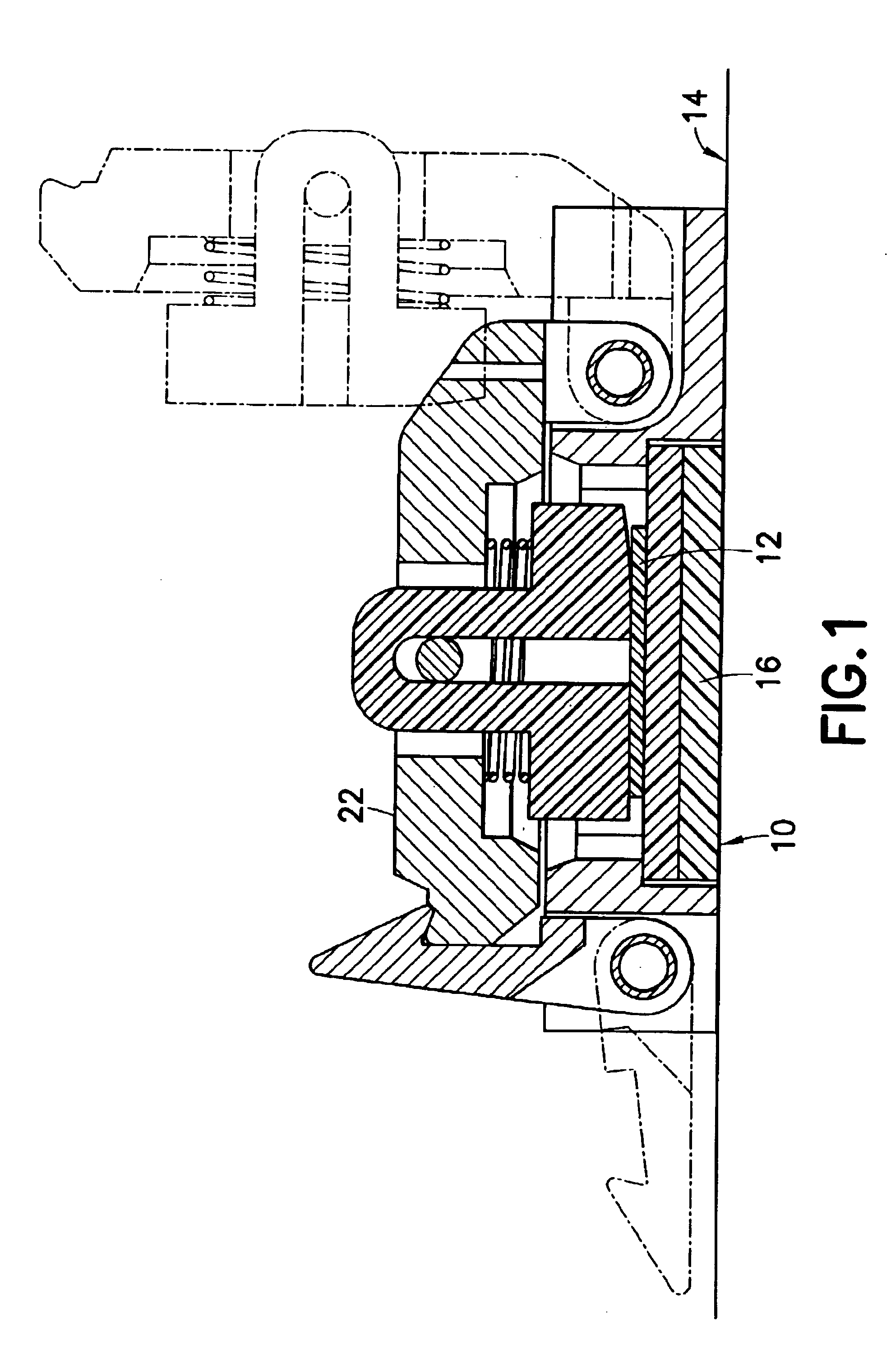
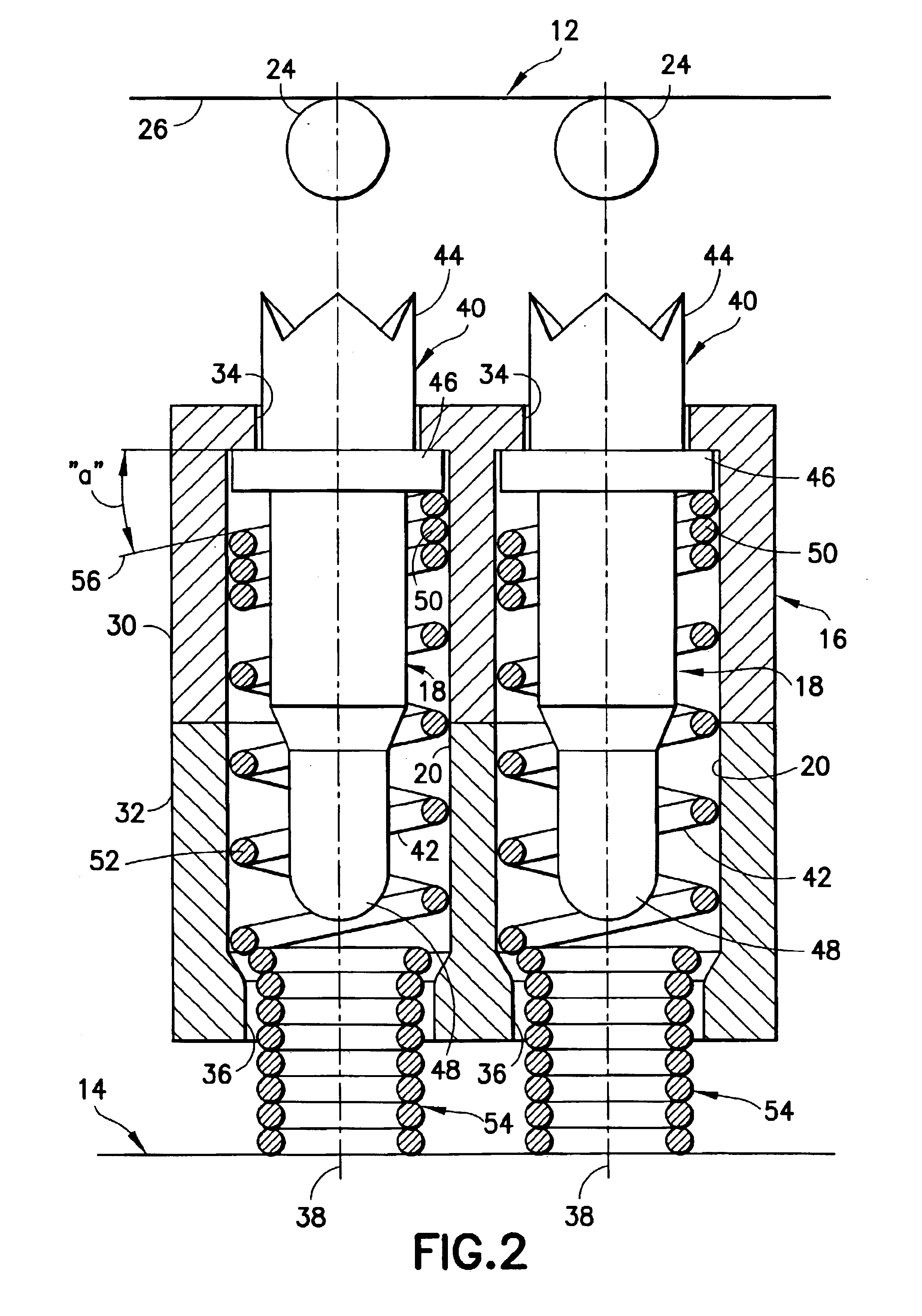
Referring to FIGS. 1-4, a new and improved connector assembly 10 is provided for connecting an IC package 12 to a printed circuit board 14. The connector 10 includes a non-conductive substrate 16 with a plurality of electrical probes 18 mounted in through holes 20 formed through the substrate 16. The number of the electrical probes 18 will generally correspond to the number of lands provided with the IC package 12. Also, the size of the connector 10 is also generally dependent on the size of the IC package 12. For purposes of illustration, the connector 10 of the subject invention will be shown and described in connection with a ball grid array (BGA) 12 package to a chip scale package (CSP) burn-in socket 22, as shown in FIG. 1.

It should be noted that the connector 10 need not be formed with the same dimensions as the IC package 12 for purposes of this invention. However, the electrical contacts 18 must be disposed in the connector 10 such that the pressing contact is achieved betwe...


PUM


Abstract

A test probe consists of an elongated screw machine contact biased by a helical spring and mounted in a through hole of a non-conductive substrate. One end of the contact includes a crown for engaging a solder ball lead of an IC package, and the contact includes an intermediate collar which maintains the contact within the through hole. The helical spring is disposed about the contact, with one end thereof engaging the lower end of the collar. The other end of the helical spring has contiguous coils and is of a reduced diameter so as to extend beyond the lower end of the non-conductive substrate to make electrical contact with a printed circuit board. When the test probe is compressed between the IC package and the printed circuit board, the inherent twisting of the helical spring causes the contact to tilt and make electrical contact with the contiguous coils, thereby establishing a direct electrical path between the IC package and the printed circuit board, with minimum resistance and minimum inductance.

Description

BACKGROUND OF THE INVENTION1. Technical FieldThe subject invention pertains generally to test probes. More specifically, the subject invention pertains to a new and improved integrated circuit (“IC”) test probe for use in various testing applications. Furthermore, the subject invention is capable of being employed in several different configurations that permit it to be used with a variety of IC chips.An electrical component, such as an IC, must be tested and evaluated for reliability before actual use. For proper testing and evaluation, the IC must be electrically connected to a printed circuit board (“PCB”) by a reliable means. As the microelectronic field has advanced, the complexity and concentration of components in an IC has increased dramatically. This increase has lead to an increased lead density of the IC chip with a corresponding decrease in the gap between the leads. Therefore, a need for smaller sized test probes to accommodate these increasingly complex ICs is needed.B...

Claims


Application Information

Patent Timeline
Patent Type & Authority Patents(United States)
IPC IPC(8): G01R1/067G01R1/02G01R1/04G01R1/073G01R31/26H01R13/15H01R13/24H01R33/76
CPCG01R1/0466G01R1/06722G01R1/07371G01R1/0483
Inventor SINCLAIR, WILLIAM Y.
Owner ARIES ELECTRONICS
Why Eureka
Try Eureka