
Active magnetic shielding

Inactive Publication Date: 2005-01-25
APPLIED MATERIALS INC
View PDF37 Cites 18 Cited by
  • Summary
  • Abstract
  • Description
  • Claims
  • Application Information

AI Technical Summary

Benefits of technology

A magnetic shield assembly which substantially surrounds a plasma region of a plasma reactor is provided. The shield assembly uses a passive shield member in combination with an active shield member. As a result, effective shielding of magnetic flux can occur without excessive distortion of the magnetic field line pattern in the plasma region.

Problems solved by technology

As a consequence, materials deposited in etched trenches and holes of semiconductor devices having trenches or holes with a high depth to width aspect ratio, can bridge over causing undesirable cavities in the deposition layer.
However in systems which employ balanced magnetrons, material sputtered in a low density plasma often has an ionization degree of less than about 5% which is usually insufficient to avoid the formation of an excessive number of cavities.
However advances in semiconductor processing designs have resulted in the need for increasingly dense plasmas.
Sometimes, such fields can extend to and interfere with adjacent equipment such as other plasma chambers or other equipment.

Method used


Image

  • Active magnetic shielding
  • Active magnetic shielding
  • Active magnetic shielding

Examples


first embodiment

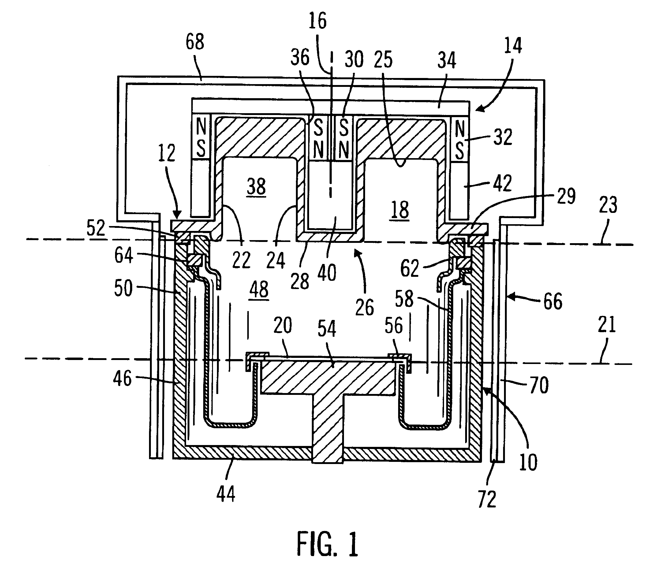
A first embodiment is illustrated by a magnetron plasma reactor 10 in the schematic cross-sectional view of FIG. 1. It includes a vault-shaped sputter target 12 and magnetron 14 symmetrically arranged about a central axis 16. The target 12 is composed of the material to be sputter deposited. The target 12 includes an annularly shaped downwardly facing vault 18 facing a wafer 20 which in turn is mounted on a semiconductor workpiece support, such as a pedestal electrode 54. The workpiece support or pedestal 54 has a generally planar support surface which is adapted to receive the wafer 20 and which defines a first imaginary plane 21 located along the axis 16. The vault 18 has an outer sidewall 22 outside of the periphery of the wafer 20, an inner sidewall 24 overlying the wafer 20, and a generally flat vault top wall or roof 25 (which closes the bottom of the downwardly facing vault 18). The vault 18 therefore defines an upper plasma region 38 for use in the sputtering process.

The tar...


PUM

PropertyMeasurementUnit
Angleaaaaaaaaaa
Angleaaaaaaaaaa
Magnetic fieldaaaaaaaaaa

Abstract

Methods and apparatuses for shielding magnetic flux which is associated with a semiconductor fabrication system are provided. A magnetic shield assembly substantially surrounds a side wall of a plasma reactor. The shield assembly comprises a passive shield member in combination with an active shield member. As a result, effective shielding of magnetic flux can occur without excessive distortion of the magnetic field line pattern in the plasma region of the plasma reactor. In one aspect, the shield assembly comprises a first shield member adapted to attenuate a magnetic flux density. The first shield member is disposed in a parallel, spaced apart relationship from the side wall. A second member is attached to the first shield member and is constructed of a ferromagnetic material which is permanently magnetized.

Description

FIELD OF THE INVENTIONThis invention relates to methods and apparatuses for sputtering a material onto a semiconductor workpiece using a plasma as part of a semiconductor fabrication system. In particular, the invention relates to magnetic shielding associated with such a fabrication system.BACKGROUNDLow density plasmas have become convenient sources of energetic ions and activated atoms which can be employed in a variety of semiconductor workpiece fabrication processes including surface treatments, depositions, and etching processes. (Semiconductor workpieces can include semiconductor wafers as well as glass compositions having semiconductor materials deposited thereon.) For example, to deposit materials onto a semiconductor wafer using a sputter deposition process, a plasma is produced in the vicinity of a sputter target material which is negatively biased. Ions created adjacent to the target impact its surface to dislodge, i.e., “sputter,” material from the target. The sputtered ...

Claims


Application Information

Patent Timeline
IPC IPC(8): H01J37/32H01J37/34
CPCH01J37/3405H01J2237/0264
Inventor PERRIN, MARK A.
Owner APPLIED MATERIALS INC
Learn More