Method of manufacturing SONOS flash memory device

a technology of sonos flash memory and manufacturing method, which is applied in the direction of semiconductor devices, basic electric elements, electrical appliances, etc., can solve the problems of cell malfunction, single-type flash memory devices cannot meet requirements for high-integration, sonos flash memory devices cannot etc., to ensure device characteristics and reliability

Inactive Publication Date: 2005-02-01
DONGBU ELECTRONICS CO LTD
View PDF7 Cites 20 Cited by
  • Summary
  • Abstract
  • Description
  • Claims
  • Application Information

AI Technical Summary

Benefits of technology

An object of the present invention is to provide a method of manufacturing a SONOS flash memory device that can prevent electrons captured in a tunnel nitride layer from traveling therein.
Another...

Problems solved by technology

However, the single type flash memory device cannot satisfy requirements for high-integration although it is a good device in itself.
However, in the conventional SONOS flash memory device, the nitride layer cannot completely prevent the electrons from traveling therein although the nitride layer is ...

Method used


Image

  • Method of manufacturing SONOS flash memory device
  • Method of manufacturing SONOS flash memory device
  • Method of manufacturing SONOS flash memory device

Examples


Embodiment Construction

Reference will now be made in detail to the preferred embodiments of the present invention, examples of which are illustrated in the accompanying drawings.

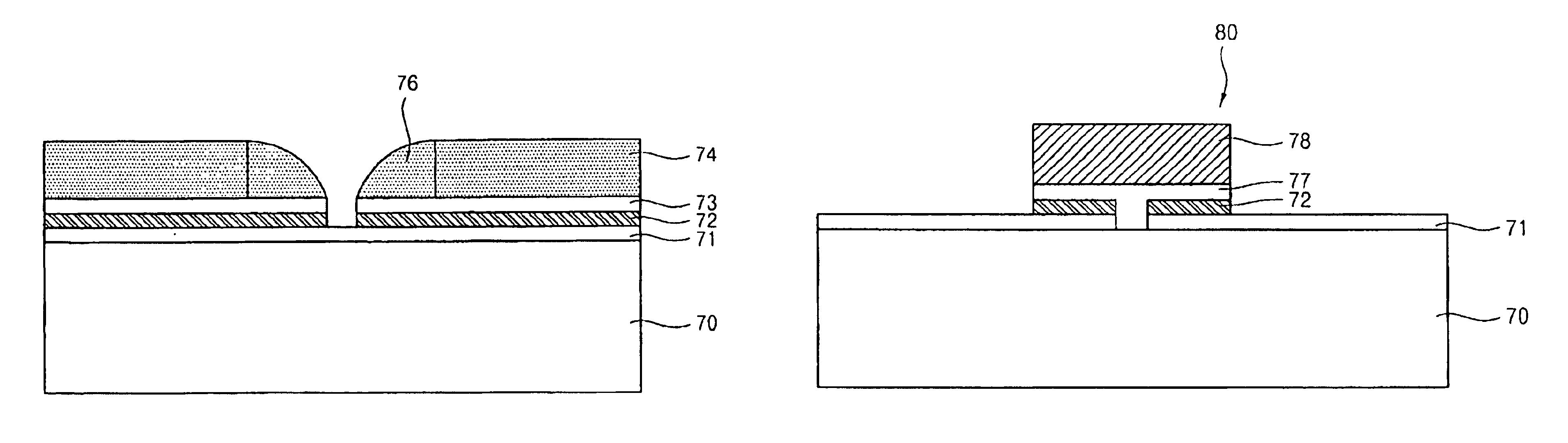
Referring to FIG. 7a, a lower oxide layer 71, a tunnel nitride layer 72, and a sacrificial oxide layer 73 are formed in sequence on a substrate 70 having device isolation layers (not shown). An insulating layer 74 for a hard mask is deposited on the sacrificial layer 73. The insulating layer 74 for a hard mask is preferably oxide or nitride formed using TEOS (tetraethyl orthosilicate) as a source.

Then, a first photoresist pattern 75 is formed on the insulating layer 74. A region for a dual bit cell is exposed by the first photoresist pattern 75. A dry-etching process is performed using the first photoresist pattern 75 as a mask to remove a portion of the insulating layer 74 for a hard mask. As a result, a portion of the sacrificial oxide layer 73 is exposed. The first photoresist pattern 75 is removed.

Referring to FIG. 7b, a first...


PUM


Abstract

A method of manufacturing a SONOS flash memory device is disclosed. The disclosed method comprises the steps of forming a lower oxide layer, a tunnel nitride layer, a sacrificial oxide layer, and an insulating layer for a hard mask in sequence on a semiconductor substrate; removing a portion of the insulating layer by an etching process; forming spacers on sidewalls of the insulating layer etched; removing some part of the sacrificial oxide layer and the tunnel nitride layer by an etching process using the insulating layer and the spacers as a mask; removing the insulating layer, the spacers, and the sacrificial oxide layer; removing a portion of the lower oxide layer by an etching process using the tunnel nitride layer etched as a mask; depositing an upper oxide layer and a polysilicon layer in sequence over the resulting structure; and forming a gate having two separate tunnel nitride layer parts by removing some parts of the polysilicon layer, the upper oxide layer, and the tunnel nitride layer in sequence by an etching process. By separating the tunnel nitride layer into two parts, movement of electrons captured in the tunnel nitride layer can be completely prevented. Therefore, the present invention can obviate device malfunction, thereby ensuring device characteristics and reliability.

Description

BACKGROUND OF THE INVENTION1. Field of the InventionThe present invention relates to a method of manufacturing a non-volatile memory device and, more particularly, to a method of manufacturing a silicon-oxide-nitride-oxide-semiconductor (SONOS) flash memory device.2. Background of the Related ArtWith the development of high-capacity memory devices, non-volatile memory devices are being increasingly important. An example of the non-volatile memory device is a flash memory device. A conventional flash memory device is a single type in which a gate structure is formed in a single cell. As shown in FIG. 1, the conventional flash memory device can indicate two states, i.e., state “1” and state “0”.However, the single type flash memory device cannot satisfy requirements for high-integration although it is a good device in itself. Thus, a multi bit cell, which has at least two gate structures in a single cell, has been developed. In addition, to embody the multi bit cell, a silicon-oxide-n...

Claims


Application Information

Patent Timeline
IPC IPC(8): H01L21/02H01L21/4763H01L21/44H01L21/336H01L21/3205H01L21/8247H01L21/28
CPCH01L21/28282H01L29/40117H10B99/00
Inventor HAN, CHANG HUN
Owner DONGBU ELECTRONICS CO LTD
Why Eureka
Try Eureka