Apparatus and process for polishing a workpiece

a technology for polishing workpieces and apparatuses, applied in metal-working apparatuses, electrical apparatus, manufacturing tools, etc., can solve the problems of reducing the mechanical strength of such devices, limiting the performance of such devices, and relatively fragile materials susceptible to shearing and crushing

Inactive Publication Date: 2005-02-01
NOVELLUS SYSTEMS
View PDF10 Cites 1 Cited by
  • Summary
  • Abstract
  • Description
  • Claims
  • Application Information

AI Technical Summary

Problems solved by technology

In the past, aluminum was used extensively as a metallization material in semiconductor fabrication due to the leakage and adhesion problems experienced with the use of gold.
As the size of integrated circuit devices becomes smaller, architectural feature restrictions, such as line isolation and material resistivity, may limit performance of such devices.
For example, the semiconductor industry has been moving to the use of copper for metallization due to the alloying and electromigration problems that are seen with aluminum.
However, such low dielectric constant materials exhibit characteristic porosity which reduces their mechanical strength, making them relatively fragile materials susceptible to shearing and crushing.
CMP may pose challenges when used for planarizing small device structures.
For example, for devices having small feature dual damascene structures, CMP may remove large areas of copper residues but also result in the over-removal of small features.
In addition, CMP may result in shearing and crushing of low dielectric constant materials.
However, the CMP process may cause cracks and loss of adhesion at the interface between the capping material and the low dielectric constant material.
Further, abrasive slurries used in CMP may result in scratching of the wafer surface, oxide erosion, dishing and the creation of defects.
The latter is particularly problematic for small structures, as a small defect will significantly jeopardize the performance of an even smaller device feature.
In addition, CMP may cause “edge effects” that reduce the die harvest from a wafer.
These edge effects are problematic as the semiconductor industry migrates from 200 mm wafers to 300 mm wafers.
With more die around the edge of a, 300 mm wafer, edge effects will result in damage to a proportionately higher number of die of the 300 mm wafer compared to a 200 mm wafer.
While exhibiting distinct advantages, abrasive-free polishing solutions may fail to provide adequate rate of removal using conventional polishing pads and delivery mechanisms.
While this conventional design may achieve acceptable rates of removal of the metal surface using an abrasive slurry, because of the chemically-reactive nature of abrasive-free polishing solutions, this conventional design does not provide for uniform distribution of the abrasive-free solution to the contact area between the wafer and the polishing pad.
The disadvantage is particularly problematic for CMP processes that require a low down force pressure of the wafer against the polishing pad.
In addition, low down force pressures may result in within-die nonuniformity.
Further, because the polishing solution is not uniformly distributed over the surface of the wafer, non-uniform planarization results.

Method used


Image

  • Apparatus and process for polishing a workpiece
  • Apparatus and process for polishing a workpiece
  • Apparatus and process for polishing a workpiece

Examples


Embodiment Construction

The following description is of exemplary embodiments only and is not intended to limit the scope, applicability or configuration of the invention in any way. Rather, the following description provides a convenient illustration for implementing exemplary embodiments of the invention. Various changes to the described embodiments may be made in the function and arrangement of the elements described without departing from the scope of the invention as set forth in the appended claims.

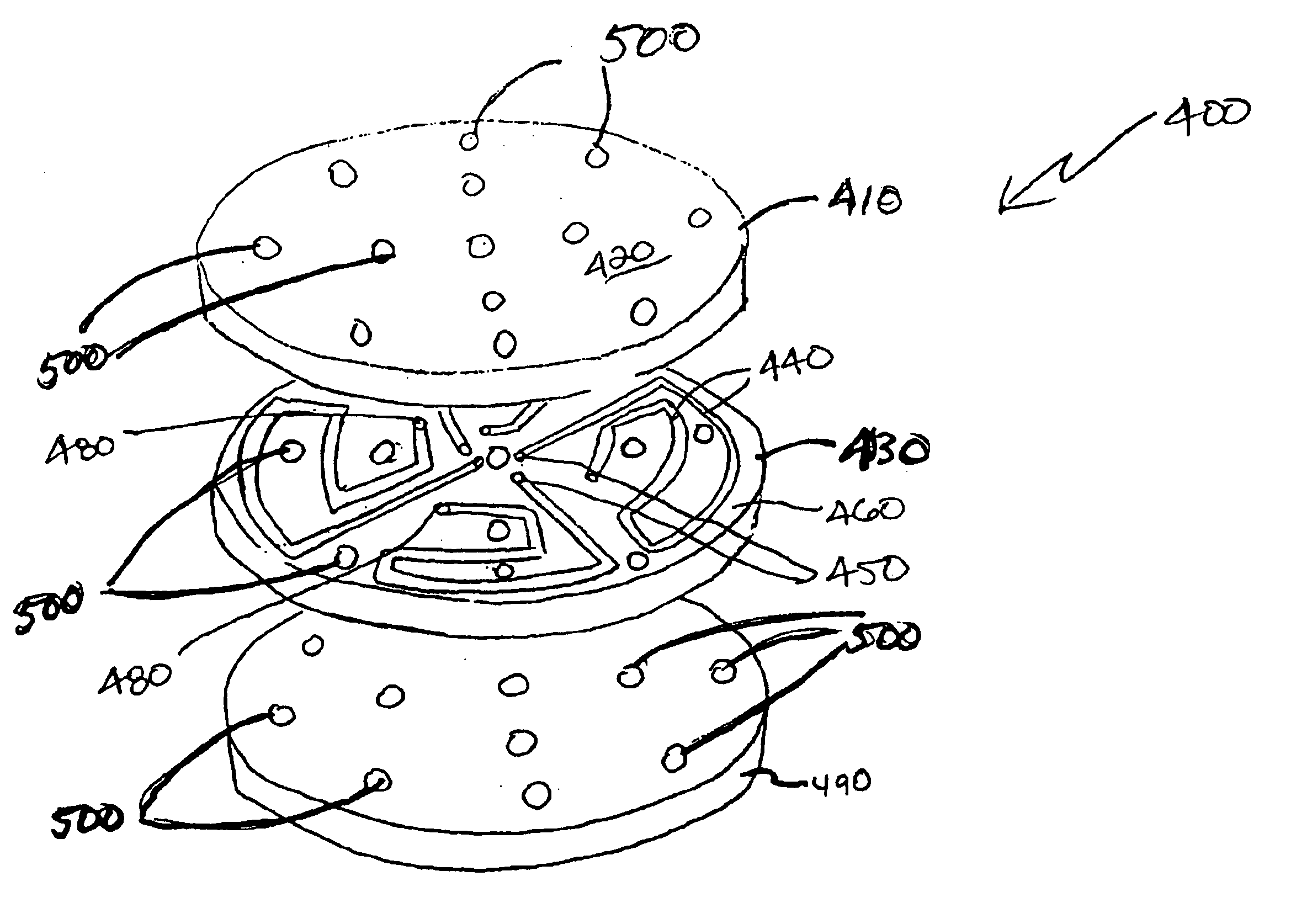
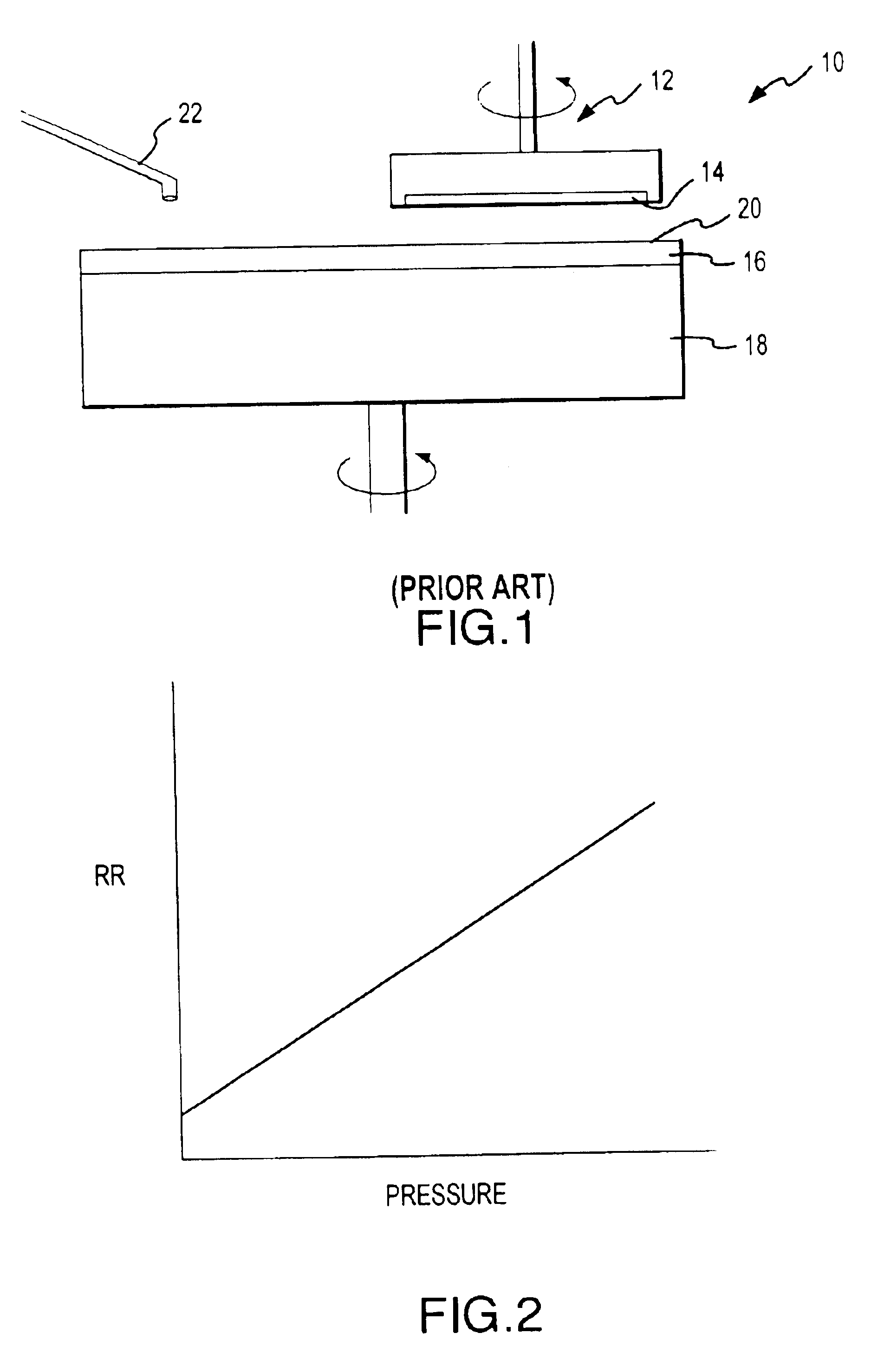
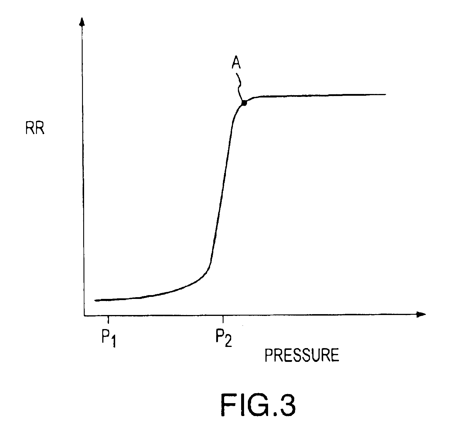
A schematic representation of an exemplary embodiment of a polishing station 100 of the present invention is shown in FIGS. 4 and 5. As herein described, polishing station 100 is configured to provide uniform and adequate distribution of an abrasive-free polishing solution so that the metallized surface of a subject workpiece readily forms a removable surface film, thereby make the abrasion step of the planarization mechanism the rate-determining step. Polishing station 100 is suitable for planarizing work...


PUM

PropertyMeasurementUnit
pressureaaaaaaaaaa
pressureaaaaaaaaaa
sizeaaaaaaaaaa

Abstract

A process for removing a metallized surface from a workpiece is provided. A kinetic removal mechanism for removal of the metallized surface is characterized by a formation step for formation of a removable surface film and an abrasive step for removal of the film. The process includes causing the workpiece to contact a polishing surface while effecting relative motion between the workpiece and the polishing surface. The process also includes causing a polishing solution having less than 1 wt % of a polishing abrasive to be distributed at a contact area between the workpiece and the polishing surface so that the abrasive step is a rate-determining step of the removal mechanism.

Description

TECHNICAL FIELDThe present invention relates, generally, to systems for polishing or planarizing workpieces, such as semiconductor wafers. More particularly, it relates to an improved method for planarizing a metallized surface on a workpiece.BACKGROUNDThe production of integrated circuits begins with the creation of high-quality semiconductor wafers. During the wafer fabrication process, the wafers may undergo multiple masking, etching, and dielectric and conductor deposition processes. In addition, metallization, which generally refers to the materials, methods and processes of wiring together or interconnecting the component parts of an integrated circuit located on the surface of a wafer, is critical to the operation of a semiconductor device. Typically, the “wiring” of an integrated circuit involves etching trenches and “vias” in a planar dielectric (insulator) layer and filling the trenches and vias with a metal.In the past, aluminum was used extensively as a metallization mat...

Claims


Application Information

Patent Timeline
Patent Type & Authority Patents(United States)
IPC IPC(8): B24B57/02B24B57/00H01L21/02H01L21/321
CPCH01L21/3212B24B57/02
Inventor CHADDA, SAKETEMESH, ISMAILMUELLER, BRIAN L.
Owner NOVELLUS SYSTEMS
Why Eureka
Try Eureka