Input/output cell with robust electrostatic discharge protection

a technology of electrostatic discharge and input/output cell, which is applied in the direction of semiconductor devices, semiconductor/solid-state device details, electrical apparatus, etc., can solve the problems of esd in electronic devices being a major obstacle to product reliability, damage to any device, and highly vulnerable to esd stress, so as to efficiently conduct large esd current and enhance esd protection

Active Publication Date: 2005-02-01
WINBOND ELECTRONICS CORP
View PDF2 Cites 21 Cited by
  • Summary
  • Abstract
  • Description
  • Claims
  • Application Information

AI Technical Summary

Benefits of technology

Due to the existence of the well stripe and the doped segment therein, there are several parasitic SCRs formed in the semiconductor device. The parasitic SCR enhances t...

Problems solved by technology

ESD in electronic devices has been a major obstacle to product reliability.
Contact with another, typically a grounded object, causes electrostatic discharge, which travels through a...

Method used


Image

  • Input/output cell with robust electrostatic discharge protection
  • Input/output cell with robust electrostatic discharge protection
  • Input/output cell with robust electrostatic discharge protection

Examples


first embodiment

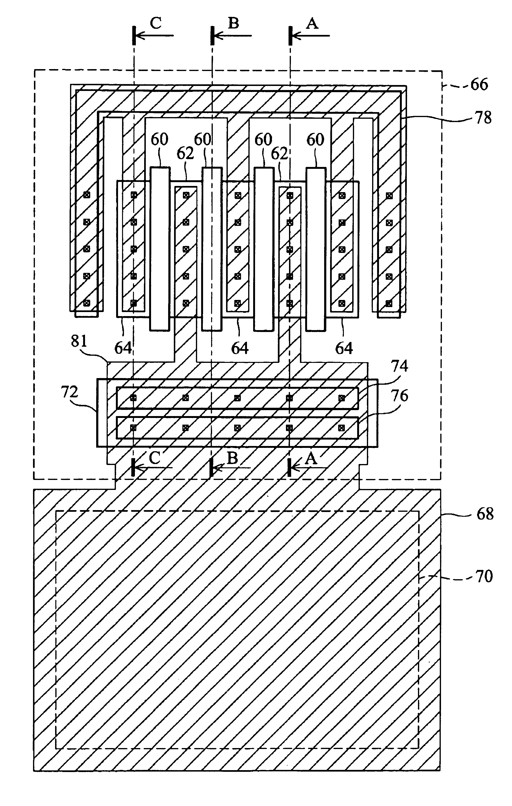
FIG. 6 depicts a layout of the present invention, including an I / O cell 66 and a pad 68. FIGS. 7A to 7C are cross sections of FIG. 6 along lines AA, BB and CC, respectively. A finger-type NMOS transistor is shown in FIG. 6 as an example. Nevertheless, this invention can also be embodied by a finger-type PMOS transistor.

In FIG. 6, the finger-type NMOS has gate fingers 60, source regions 64 and drain regions 62. The finger-type NMOS transistor is formed in an active region substantially surrounded by an isolation region. Source regions 64 and drain regions 62 are of N-type. Through contacts and metal wires, source regions 64 are connected to a power rail, VSS, and drain regions 62 to pad 68, on which an opening 70 is formed in a passivation layer (not shown). Each gate finger 60 is located on a channel region between one source region 64 and one drain region 62. Gate fingers 60 are substantially parallel to each other. Gate fingers 60 can be connected either to a pre-driver to serve a...

second embodiment

FIG. 8 depicts a layout of the present invention. FIGS. 9A to 9C are cross sections of FIG. 8 along lines AA, BB and CC, respectively. The finger-type NMOS can be replaced by a field device. Gate fingers in FIG. 6 are replaced by a field-oxide-isolation stripe such as the STI regions in FIG. 8. FIGS. 9A and 9C are the same with FIGS. 7A and 7C. In FIG. 9B, an STI region 84 is formed on a channel region 82. The operation principle during an ESD event for the semiconductor device in FIG. 8 is substantially the same as that for the semiconductor device in FIG. 6.

The pattern in N-well stripe 72 can be altered. For example, FIG. 10 shows that one N+ region is divided into a number of separate N+ sub-regions 761. Separate N+ sub-regions 761 provide a contact region with less area than one N+ region 76 and forms a resistor with higher resistance to conduct the electron flow after parasitic BJTs go into snapback. This resistor with higher resistance will lower the SCR trigger current.

FIG. 1...


PUM


Abstract

An electrostatic discharge (ESD) protection device with enhanced ESD robustness. The ESD protection device comprises a pad, a finger-type MOS, a well stripe and a doped segment. The pad is on a semiconductor substrate of a first-conductive type. The finger-type MOS is on the semiconductor substrate and comprises drain regions, source regions and channel regions. Each drain region is of a second-conductive type and is coupled to the pad. Each source region is of the second-conductive type and coupled to a power rail. Channel regions are formed on the semiconductor, substantially parallel to each other. Each channel region is located between one source region and one drain region. The well stripe is of the second-conductive type and formed on the semiconductor, in an angle to the channel regions. The doped segment is of the first-conductive type and in the well stripe. Furthermore, the doped segment is coupled to the pad.

Description

BACKGROUND OF THE INVENTION1. Field of the InventionThe present invention relates to an electrostatic discharge (ESD) protection device in an integrated circuit (IC). In particular, the present invention relates to an input / output (I / O) cell capable of uniform ESD current discharge during an ESD event.2. Description of the Related ArtESD in electronic devices has been a major obstacle to product reliability. Electrostatic charge can accumulate in a human body, a machine or an electric device of up to several thousand volts. Contact with another, typically a grounded object, causes electrostatic discharge, which travels through a path and may damage any device along the path if the device is not well protected.There are several known test models, such as Human Body Mode (HBM), Machine Mode (MM), and others, to simulate different conditions under which ESD occurs. An electronic device can only be certified for commercialized after passing tests of a certain level for each test model.E...

Claims


Application Information

Patent Timeline
IPC IPC(8): H01L23/58H01L23/62H01L23/60H01L27/02
CPCH01L27/0266H01L2924/0002H01L2924/00
Inventor LIN, SHI-TRON
Owner WINBOND ELECTRONICS CORP
Why Eureka
Try Eureka