Thin film transistor organic light emitting diode structure

a thin film transistor and organic light-emitting diode technology, applied in the direction of discharge tube luminescnet screens, identification means, instruments, etc., can solve the problems of difficult control of surface rough difficult to produce the desired flatness of the anode layer, etc., to achieve the effect of lowering the power demand of the el display device and reducing the contact resistance between the anode and the source electrod

Inactive Publication Date: 2005-02-01
AU OPTRONICS CORP
View PDF5 Cites 40 Cited by
  • Summary
  • Abstract
  • Description
  • Claims
  • Application Information

AI Technical Summary

Benefits of technology

[0013]Next, the EL element's anode is deposited on the substrate so that a portion of the EL element's anode overlaps and enshrouds the portion of the TFT's source electrode that is directly on the substrate. An important feature of this resulting structure is that the TFT's source electrode and the EL element's anode contact each other at the overlapping region without any intervening structure or materials therebetween. During the process of forming the TFT on the substrate, the source electrode is deposited with a portion directly on the substrate. The EL element's anode is, then, deposited on the substrate near the TFT so that an edge portion of the anode overlaps the source electrode and enshrouds an edge surface of the source electrode. The anode contacts the edge surface and the top surface of the source electrode. The result is that the contact area between the anode and the source electrode is larger than the contact made through a contact via hole in the conventional structures. Hence, the contact resistance between the anode and the source electrode is lower and, in turn, lowering the power demand of the EL display device. In another embodiment of the present invention, the order of depositing the EL element's anode and the TFT's source electrode may be reversed. The EL element's anode may be deposited first on the substrate and the TFT's source electrode is deposited with a portion directly on the substrate and overlapping the EL element's anode.

Problems solved by technology

Another problem with the conventional EL display device structure is that it is difficult to produce an anode layer having a desired flatness.
Because the anode 210 of the EL element is deposited over a number of underlying layers of insulation films, it is difficult to control the surface roughness of the anode layer.

Method used


Image

  • Thin film transistor organic light emitting diode structure
  • Thin film transistor organic light emitting diode structure
  • Thin film transistor organic light emitting diode structure

Examples


Embodiment Construction

_n">[0019]FIG. 3 is a schematic cross-sectional view of an improved EL display device according to another embodiment of the present invention; and

[0020]FIG. 4 is a schematic cross-sectional view of the contact region between a TFT's source electrode and an EL element's anode according to another embodiment of the present invention.

[0021]Same reference numerals are used to denote like parts throughout the various figures.

DETAILED DESCRIPTION

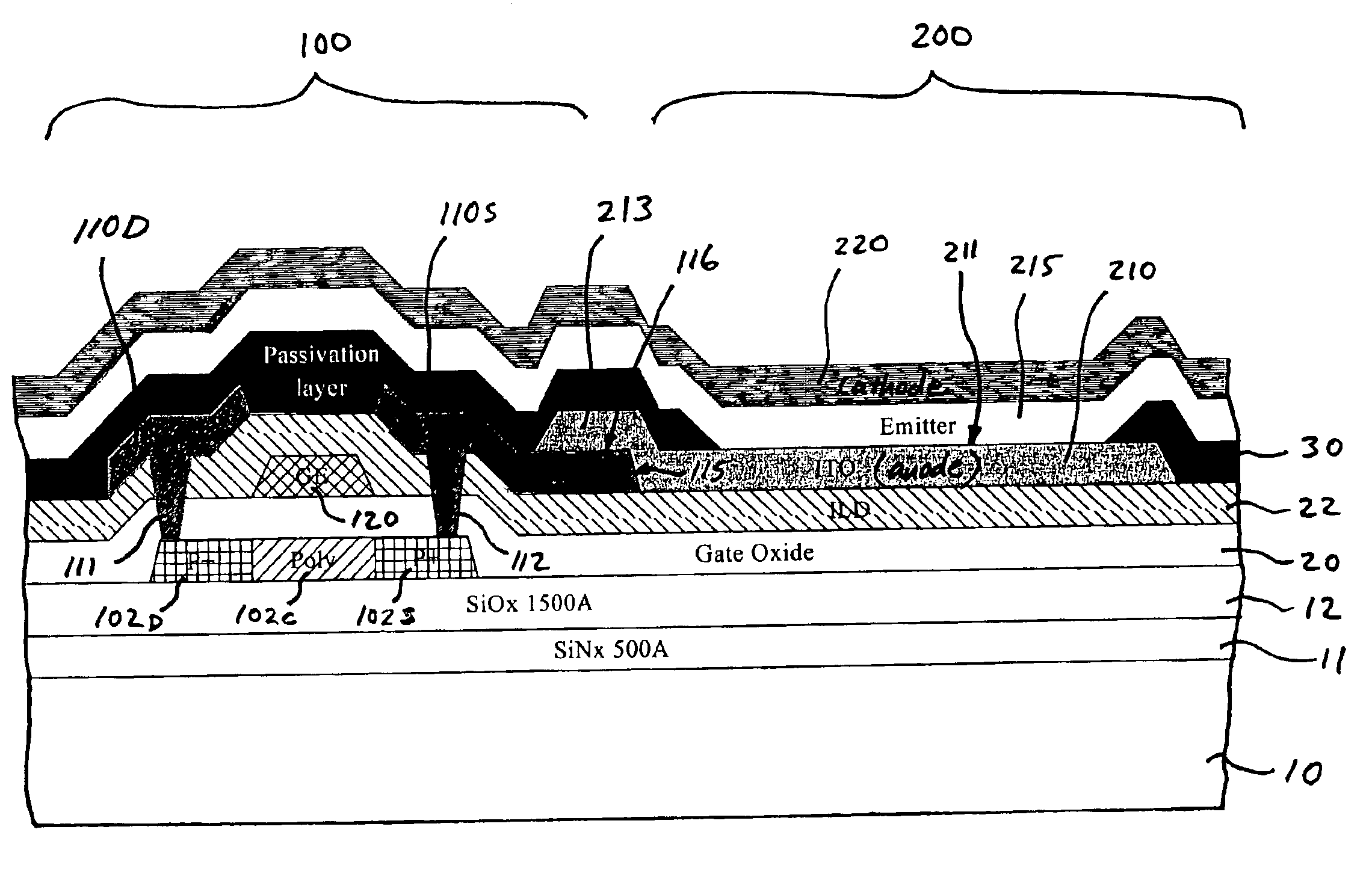
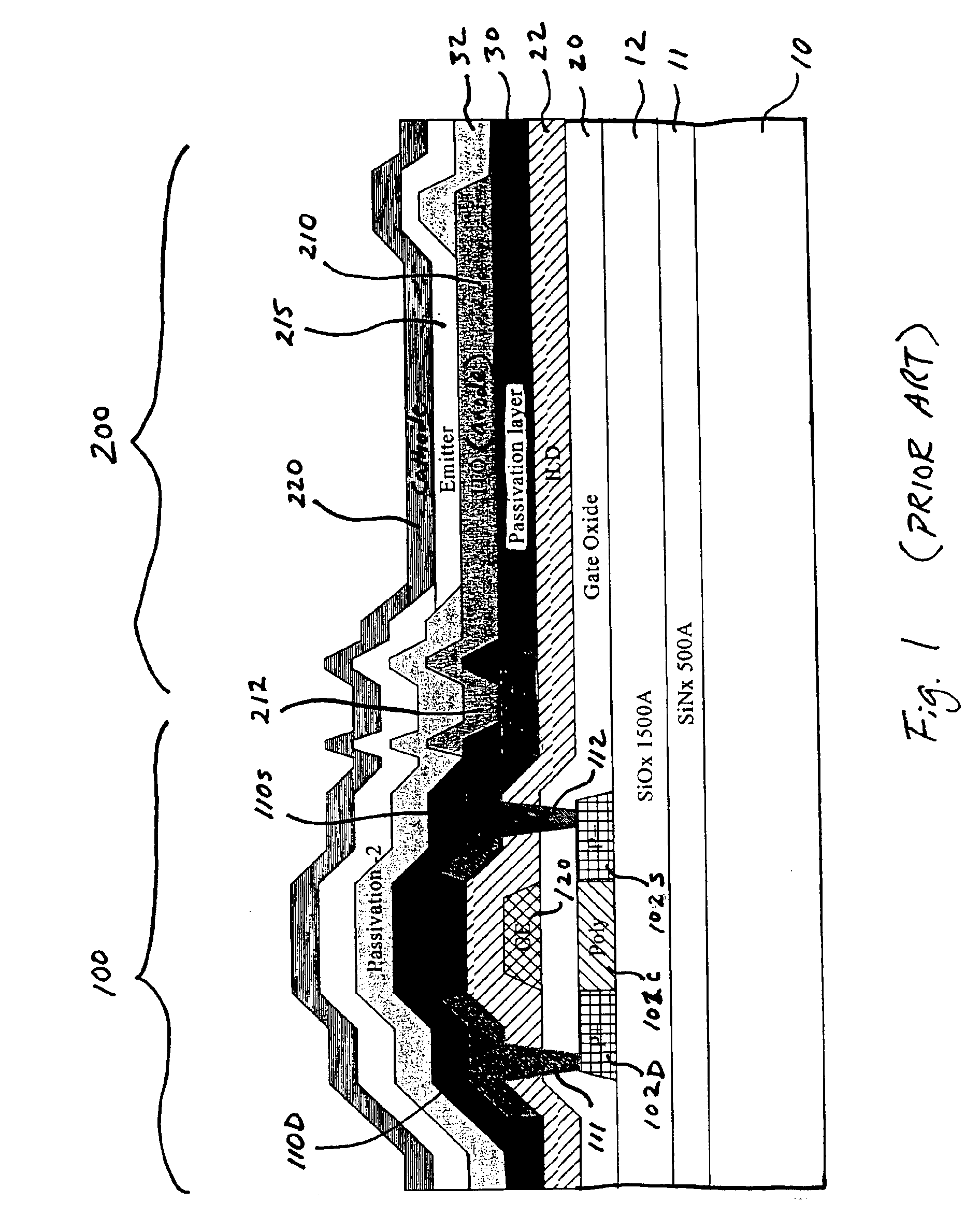
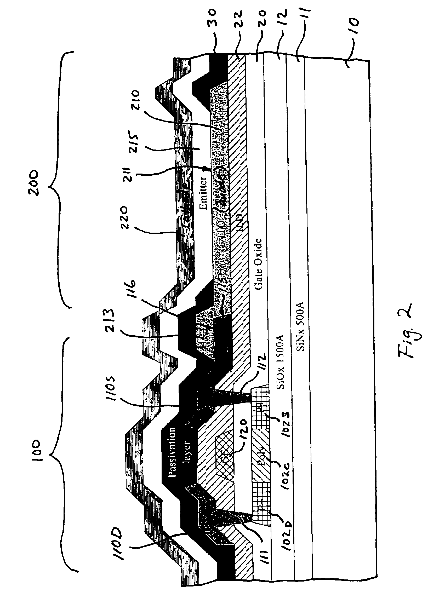
[0022]Referring to FIG. 2, an improved electroluminescence (EL) display device according to an embodiment of the present invention is disclosed. The EL display device comprises a thin-film-transistor (TFT) and an EL element 200 formed on a substrate 10. The EL element in this embodiment is an organic light emitting diode and the TFT is used to drive the EL element 200. The substrate 10 is transparent and may be formed of a non-conductive material, such as, glass, synthetic resin, or the like. It may also be formed of a conductive or semiconductor...


PUM


Abstract

An electroluminescence display device comprising a thin film transistor and an electroluminescence element wherein the electroluminescence element's anode and a portion of the thin film transistor's source/drain electrode are deposited on to a same surface and the electroluminescence element's anode and the portion of the thin film transistor's source/drain electrode overlap and make an electrical contact with improved contact resistance.

Description

FIELD OF THE INVENTION[0002]The present invention relates to an electroluminescence (EL) display device, and more particularly to an EL display device comprising an EL element and a thin film transistor (TFT) that is employed as a switching element for the EL element.BACKGROUND OF THE INVENTION[0003]In a conventional EL display device, such as a TFT Organic Light Emitting Diode (TFT-OLED), one of the electrodes of the EL element contacts either the source or the drain electrode of the associated TFT device through a contact via hole in the underlying passivation layer. For example, schematically illustrated in FIG. 1 is a cross-sectional view of a conventional TFT-OLED device. The TFT-OLED device is composed of a TFT device 100 and an OLED device 200 that are formed on top of a substrate 10. The substrate 10 in this example is a semiconductor material and, thus, insulating buffer films 11 and 12 of silicon nitride and silicon oxide, respectively, are first formed on the substrate 10...

Claims


Application Information

Patent Timeline
Patent Type & Authority Patents(United States)
IPC IPC(8): G09G3/10G09G3/04G09F9/30H05B33/14H05B33/26H05B33/12H01L51/50H01L27/32
CPCH01L27/3248H10K59/123
Inventor HUANG, WEI-PANGCHEN, JUI-HSINGLEE, HSIN-HUNG
Owner AU OPTRONICS CORP
Why Eureka
Try Eureka