Semiconductor memory device with reduced current consumption during standby state

a memory device and semiconductor technology, applied in the direction of information storage, static storage, digital storage, etc., can solve the problems of dram being identified as a defective product, affecting the quality of dram, so as to achieve the effect of reducing current consumption

Inactive Publication Date: 2005-02-01
RENESAS TECH CORP
View PDF6 Cites 52 Cited by
  • Summary
  • Abstract
  • Description
  • Claims
  • Application Information

AI Technical Summary

Benefits of technology

[0015]It is an object of the present invention to provide a semiconductor memory device capable of reducing current consumption in a standby state.

Problems solved by technology

However, these Prior Art Documents 1 and 2 fail to consider the current consumption due to the existence of a leakage path caused by a particle (contaminant) such as etching residue in a manufacturing process.
When this short circuit is low-resistive, the selected word line is not driven to a select state in the DRAM or the voltage level of the bit line is fixed by the unselected word line, thus causing malfunctions such as a state where memory cell data cannot be read.
As a result, the DRAM is identified as a defective product during a test.
In this case, the quantity of a leakage current through the high resistance becomes significantly innegligible.

Method used


Image

  • Semiconductor memory device with reduced current consumption during standby state
  • Semiconductor memory device with reduced current consumption during standby state
  • Semiconductor memory device with reduced current consumption during standby state

Examples


first embodiment

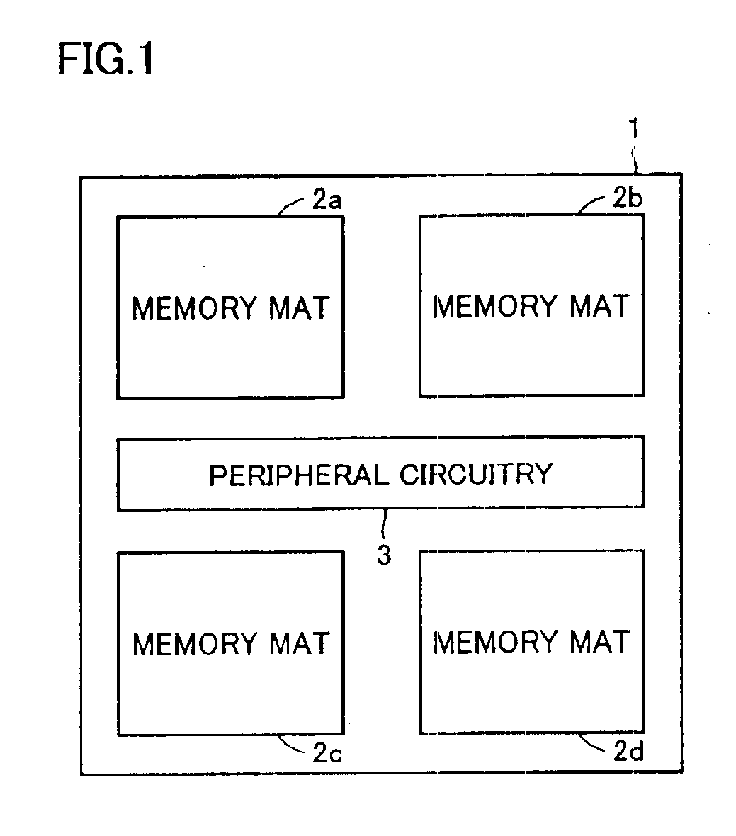
[0046]FIG. 1 is a schematic diagram showing an overall configuration of a semiconductor memory device according to the present invention. In FIG. 1, semiconductor memory device 1 includes memory mats 2a to 2d arranged being distributed in four-divided regions, and peripheral circuitry 3 arranged in the region between memory mats 2a and 2b and memory mats 2c and 2d.

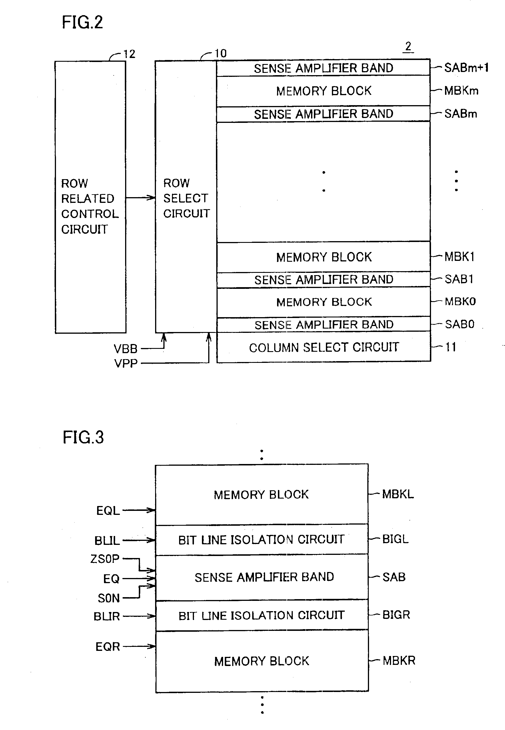
[0047]Each of memory mats 2a to 2d includes a memory array having a plurality of memory cells arranged in rows and columns, a row select circuit selecting a memory cell row, and a column select circuit selecting a memory cell column. In each of memory mats 2a to 2d, memory cells are arranged being divided into a plurality of memory blocks, and sense amplifier bands are arranged, corresponding to the memory blocks, such that a sense amplifier is shared between a memory block and an adjacent memory block.

[0048]Peripheral circuitry 3 includes an input / output circuit inputting and outputting data, an input buffer receiving an...

second embodiment

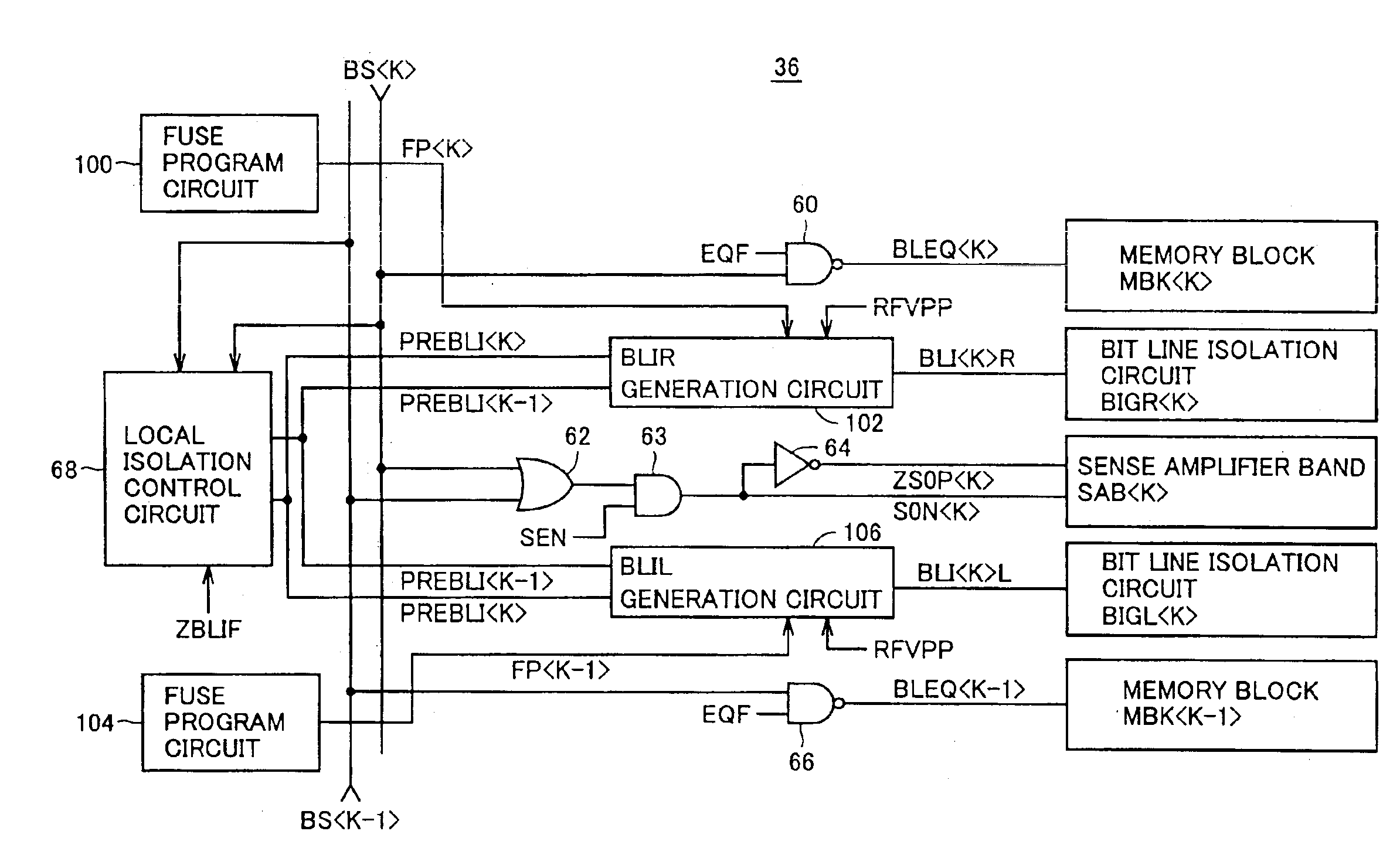
[0201]FIG. 23 is a schematic diagram showing the configuration of the row related local control circuit according to a second embodiment of the present invention. Row related local control circuit 36 shown in FIG. 23 differs in configuration from row related local control circuit 36 shown in FIG. 16 in the following points. Fuse program circuits 100 and 104 are provided in correspondence to memory blocks MBK and MBK, respectively. Data as to whether a short circuit exists between the bit line and the word line in corresponding memory blocks MBK or MBK is programmed in each of fuse program circuits 100 and 104 by blow / non-blow of a link element.

[0202]A BLIR generation circuit 102 which generates bit line isolation instruction signal BLIR selects either pre-bit line isolation control signal PREBLI or PREBLI applied from local isolation control circuit 68 in accordance with program data FP from fuse program circuit 100 and isolation control switch signal RFVPP, and generates bit line i...


PUM


Abstract

Data indicating whether a short-circuit defect exists in a memory block is programmed a fuse program circuit. In accordance with the fuse program data and a mode instruction signal, the correspondence relationship between a block select signal and a corresponding bit line isolation instruction signal is switched by a circuit that generates the bit line isolation instruction signal in a specific mode. It becomes possible to isolate the memory block in which a leakage current path exists from a corresponding sense amplifier band in a specific operation mode. Current consumption at least at a standby state is reduced.

Description

BACKGROUND OF THE INVENTION[0002]1. Field of the Invention[0003]The present invention relates to a semiconductor memory device and, particularly, to a dynamic type semiconductor memory device that requires a refresh operation for data retention. More specifically, the present invention relates to a configuration for reducing current consumption during a stand-by state, particularly, in a data holding mode.[0004]2. Description of the Background Art[0005]In a dynamic semiconductor memory device (DRAM: Dynamic Random Access Memory), data is stored in a capacitor in the form of charges. At accessing of data in a memory cell, the charges stored in the capacitor are read to a corresponding bit line. The bit line is precharged at a predetermined voltage level in a standby state. A sense amplifier provided in correspondence to the bit line detects the voltage change generated on the bit line and the memory cell data is read. The voltage of the bit line fully swings by the amplification oper...

Claims


Application Information

Patent Timeline
Patent Type & Authority Patents(United States)
IPC IPC(8): G11C11/401G11C11/4091G11C7/00G11C8/00G11C11/409G11C11/34G11C11/403G11C11/406G11C7/12G11C11/4094G11C29/00
CPCG11C7/12G11C11/4094G11C29/832G11C29/83G11C2207/2227
Inventor KUGE, SHIGEHIROHAMAMOTO, TAKESHI
Owner RENESAS TECH CORP
Why Eureka
Try Eureka