Semiconductor memory device having ECC type error recovery circuit

a memory device and error recovery technology, applied in the field of semiconductor memory devices, can solve the problems of large chip size, large circuit scale of ram devices, and large chip size of rom devices, and achieve the effects of easy measurement, easy reading out, and poor reading out speed of cell data

Inactive Publication Date: 2005-02-01
RENESAS ELECTRONICS CORP
View PDF13 Cites 120 Cited by
  • Summary
  • Abstract
  • Description
  • Claims
  • Application Information

AI Technical Summary

Benefits of technology

It is another object of the present invention to provide a semiconductor memory device having an ECC type error recovery circuit in which the worst reading out speed of cell data can be easily measured form outside.
It is another object of the present invention to provide a semiconductor memory device having an ECC type error recovery circuit in

Problems solved by technology

This is because, when the ECC type error recovery circuit is used in a RAM device, a circuit scale of the RAM device becomes very large.
On the other hand, when the redundancy cell type error recovery circuit is used in a ROM device, the chip size of the ROM device becomes large.
Therefore, the chip size becomes large.
In the conventional memory device which uses the ECC type error recovery circuit, there is a disadvantage as follows.
In such conventional memory device, it is impossible to correctly measure from outside the worst value of reading out speed of cell data.
However, in recent memory devices, memory capacities have become larger than before, and, therefore, error recovery circuits such as the above-mentioned ECC type error recovery circuits have become essential for the memory devices.
Also, a rising (or falling) time of a word select signal becomes slow at the far end portion of a word line when compared with that at the near end portion on the side of an X address decoder, and, therefore, a read out speed of cell data becomes slow at the far end portion of a word line.
However, it is impossible to measure the read out speed of the ECC cells.
Th

Method used


Image

  • Semiconductor memory device having ECC type error recovery circuit
  • Semiconductor memory device having ECC type error recovery circuit
  • Semiconductor memory device having ECC type error recovery circuit

Examples


Embodiment Construction

With reference to the drawings, embodiments of the present invention will be described in detail.

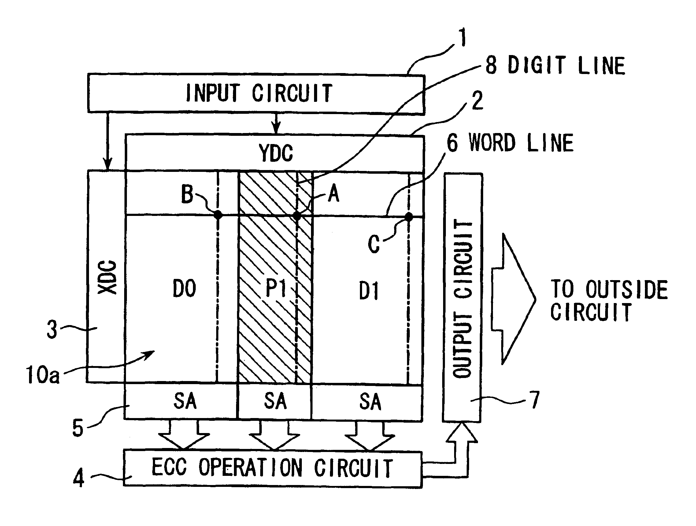
FIG. 1 is a layout diagram showing a structure of a memory device having an ECC type error recovery circuit according to an embodiment of the present invention. The memory device of FIG. 1 comprises a memory cell array 10a having a large number of memory cells (not shown in the drawing) which are disposed in a matrix and each of which is disposed at an intersection of a word line 6 and a digit line 8. The memory device of FIG. 1 further comprises an input circuit 1, a Y address decoder (or Y address decoding circuit: YDC) 2, an X address decoder (or X address decoding circuit: XDC) 3, an ECC operation circuit 4, sense amplifier blocks (SA) 5, and an output circuit 7.

The memory cell array 10a comprises normal cell array portions D0 and D1 and an ECC cell array portion P1. In FIG. 1, only two normal memory cell array portions D0 and D1 are shown. However, the number of the normal cell arra...


PUM


Abstract

A semiconductor memory device having an error check and correction (ECC) type error recovery circuit in which disposition of ECC cells is improved. The memory device comprises: a memory cell array including a plurality of normal cell array portions and an ECC cell array portion; an X decoder for selecting one of word lines in the memory cell array, the word lines extending from the X decoder to the memory cell array; an ECC operation circuit for performing error check and correction based on cell data read out from a selected word line, the cell data including data from normal cells and ECC cells of the selected word line. The ECC memory cell array portion is disposed at a location other than the far end of the word lines from the X decoder, that is, the ECC cell array portion is disposed at a location in which read out speed of data from ECC cell or cells does not become the worst speed in the memory device. Therefore, the worst data read out speed can be measured from outside.

Description

FIELD OF THE INVENTIONThe present invention relates generally to a semiconductor memory device, and more particularly to a semiconductor memory device having an error check and correction (ECC) type error recovery circuit in which disposition of ECC cells in a memory cell array is improved.BACKGROUND OF THE INVENTIONAccording to an increase in memory capacity of a semiconductor memory device, it becomes indispensable to use an on-chip error recovery circuit which recovers or relieves error of defective memory cells. Typical error recovery circuits include a redundancy cell type error recovery circuit and an ECC type (or an ECC cell type) error recovery circuit.The semiconductor memory device with a redundancy cell type error recovery circuit has normal memory cells and spare or redundant memory cells. When an address sent to a memory device is for a line, that is, a digit line or a word line, on which faulty cell or cells reside, the address decoder for the redundant line activates ...

Claims


Application Information

Patent Timeline
IPC IPC(8): G11C29/42G11C29/04G06F11/10G11C29/00G06F12/16
CPCG06F11/1008G11C29/42G06F2211/109G11C29/00
Inventor YAMAMOTO, KOUJI
Owner RENESAS ELECTRONICS CORP
Why Eureka
Try Eureka