Conductive through wafer vias

a technology of conductive through wafer and via, which is applied in the direction of printed element electric connection formation, liquid/fluent solid measurement, instruments, etc., can solve the problems of adversely affecting the conductivity of the contacts, difficult conformal filling of high aspect ratio vias, and limited methods of filling through vias using plasma chemical vapor deposition process to form seed layer followed by conformal metal electroplating process, etc. cost saving

Inactive Publication Date: 2005-02-08
MICRON TECH INC
View PDF20 Cites 85 Cited by
  • Summary
  • Abstract
  • Description
  • Claims
  • Application Information

AI Technical Summary

Benefits of technology

The invention advantageously provides a simplified method of forming through-wafer vias that are void-free. The present method involves fewer process steps than prior art methods, provides a c...

Problems solved by technology

Conventional methods of filling a through-via using a plasma chemical vapor deposition (PCVD) process to form a seed layer followed by a conformal metal electroplating process are limited to low ...

Method used


Image

  • Conductive through wafer vias
  • Conductive through wafer vias
  • Conductive through wafer vias

Examples


Embodiment Construction

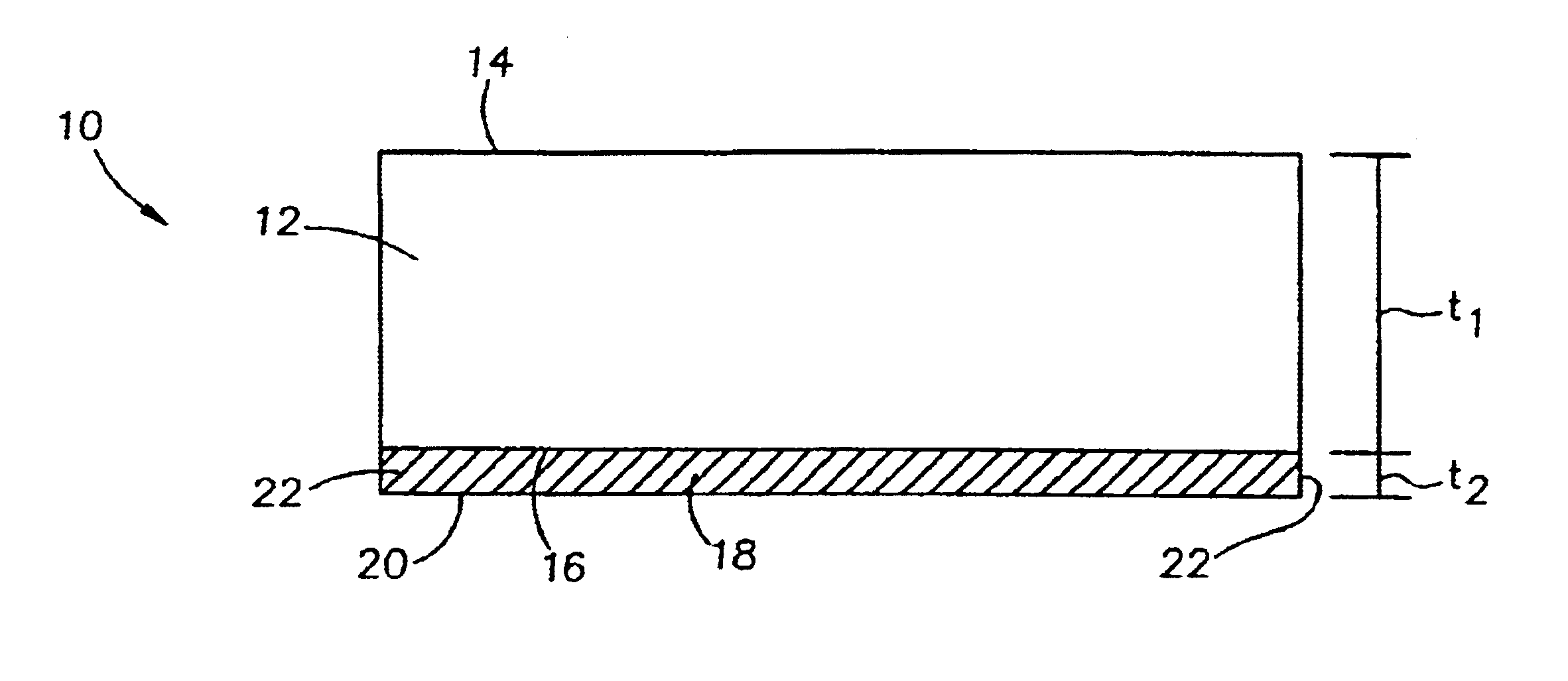
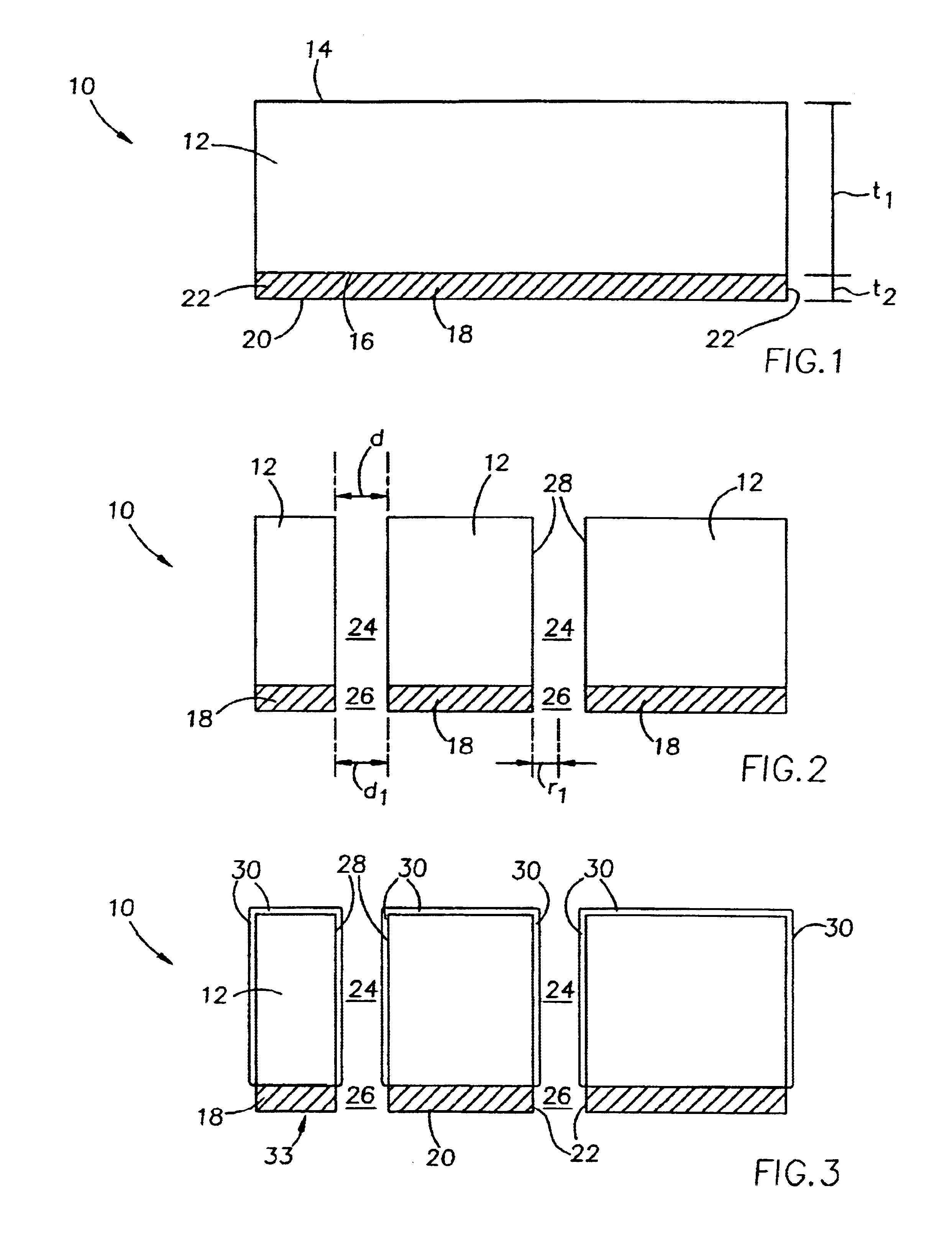
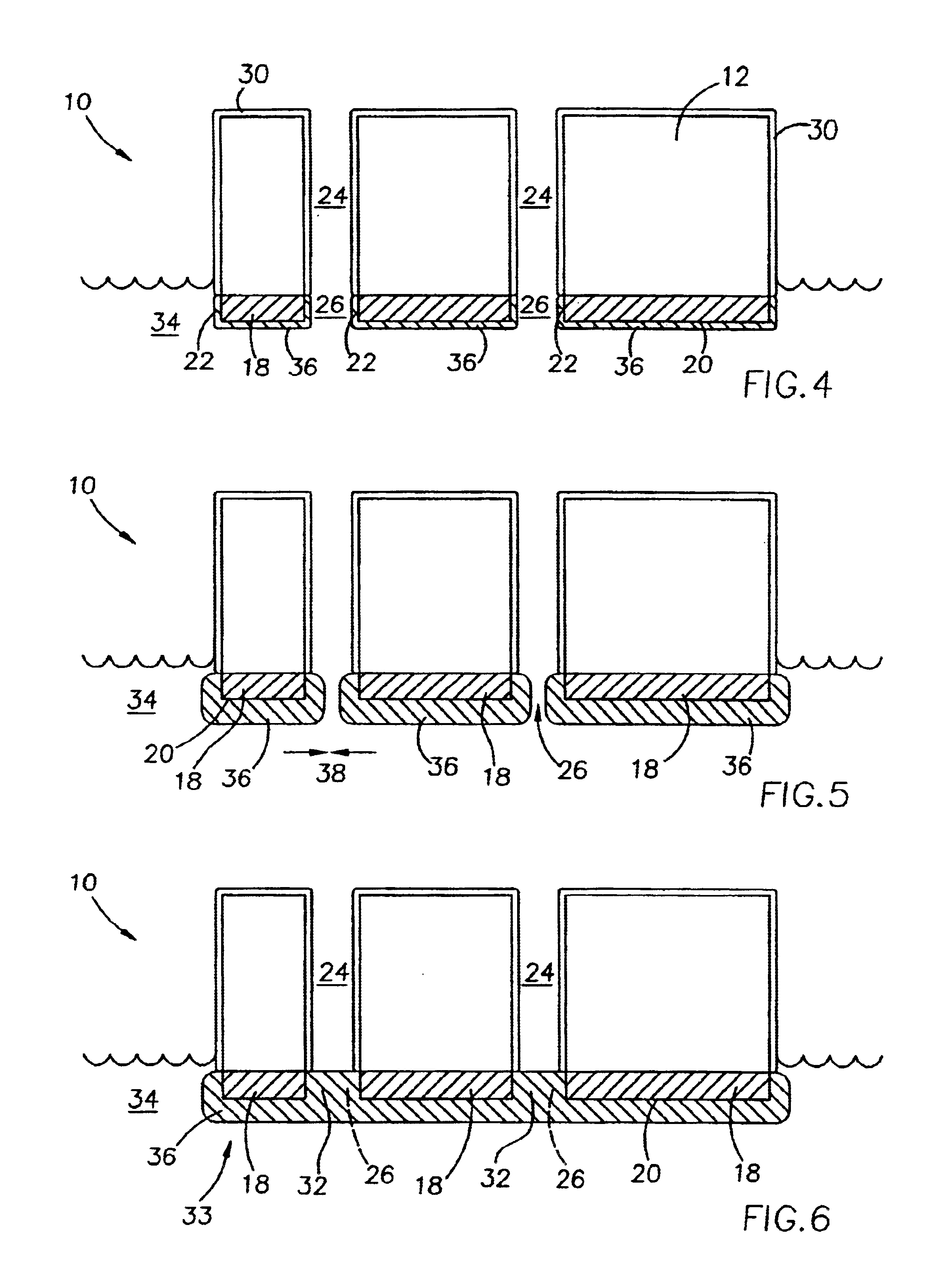
The invention will be described generally with reference to the drawings for the purpose of illustrating the present preferred embodiments only and not for purposes of limiting the same. The figures illustrate processing steps for use in fabricating a conductive through-via in accordance with the present invention. It should be readily apparent that the processing steps are only a portion of the entire fabrication process.

In the current application, the terms “semiconductive wafer fragment” or “wafer fragment” or “wafer” will be understood to mean any construction comprising semiconductor material, including but not limited to bulk semiconductive materials such as a semiconductor wafer (either alone or in assemblies comprising other materials thereon), and semiconductive material layers (either alone or in assemblies comprising other materials). The term “substrate” refers to any supporting structure including, but not limited to, the semiconductive wafer fragments or wafers describ...


PUM


Abstract

Methods for fabricating a conductive contact (through-via) through a full thickness of a substrate such as a semiconductor wafer or interposer substrate, and semiconductor devices and systems incorporating the conductive through-via are provided. The conductive contact is fabricated by applying a metal layer onto a backside of a substrate, forming a through-hole through the substrate and the metal layer, sealing the hole in the metal layer by an electroless plating process, and filling the hole by an electroplating or an electroless plating process.

Description

FIELD OF THE INVENTIONThe invention relates generally to semiconductor fabrication, and more particularly to methods for providing interconnects from one surface to the opposite surface of a substrate for making electrical connections with semiconductor components, and more particularly to methods for filling a through-via in a wafer, interposer or other substrate with a conductive material.BACKGROUND OF THE INVENTIONInterposers are utilized for interfacing two electrical components, for example, a semiconductor device and a printed circuit board, or a semiconductor wafer and a probe card for testing of the dies on the wafer. These interposers may comprise silicon or ceramic substrate that include metal-filled vias that extend through the interposer from one side to the opposite side. The metal-filled via provide electrical communication between conductive structures disposed on the opposing surfaces of the interposer, which align with contact pads or other structures of the electri...

Claims


Application Information

Patent Timeline
IPC IPC(8): H01L21/70H01L21/02H01L23/48H01L21/48H01L21/768H05K3/42H01L23/498H05K3/24
CPCH01L21/486H01L21/76898H01L23/481H05K3/422H01L23/49827H01L2924/09701H05K3/244H01L2924/0002H05K3/426H05K3/427H05K2201/0394H01L2924/00H01L2224/02372H01L21/2885H01L21/76879
Inventor SINHA, NISHANTFARNWORTH, WARREN M.
Owner MICRON TECH INC
Why Eureka
Try Eureka