Nano-architected/assembled solar electricity cell

Inactive Publication Date: 2005-02-08
AERIS CAPITAL SUSTAINABLE IP
View PDF20 Cites 348 Cited by
  • Summary
  • Abstract
  • Description
  • Claims
  • Application Information

AI Technical Summary

Benefits of technology

The disadvantages associated with the prior art are over come by a solar cell device architecture wherein two different materials are regularly arrayed and wherein the presence of two different materials alternates within 1 nm to 100 nm distances. The two materials may be arrayed using nanostructures such as filled pores, nanolamellas, or other matrixed nanostructures. The architecture integrates a conducting or semiconducting polymer into a mesoporous substrate to form a base matrix for a nanostructured layer. The architecture may be implemented with a mesoporous template having a conducting or semiconducting polymer or other media containing pores that are filled with a material having a different electron affinity than the surrounding conducting or semiconducting media to create an interdigitated mesh network amongst the conducting or semiconducting polymer media.

Problems solved by technology

The disadvantages associated with the prior art are over come by a solar cell device architecture wherein two different materials are regularly arrayed and wherein the presence of two different materials alternates within 1 nm to 100 nm distances.

Method used


Image

  • Nano-architected/assembled solar electricity cell
  • Nano-architected/assembled solar electricity cell
  • Nano-architected/assembled solar electricity cell

Examples


Embodiment Construction

Although the following detailed description contains many specific details for the purposes of illustration, anyone of ordinary skill in the art will appreciate that many variations and alterations to the following details are within the scope of the invention. Accordingly, the exemplary embodiments of the invention described below are set forth without any loss of generality to, and without imposing limitations upon, the claimed invention.

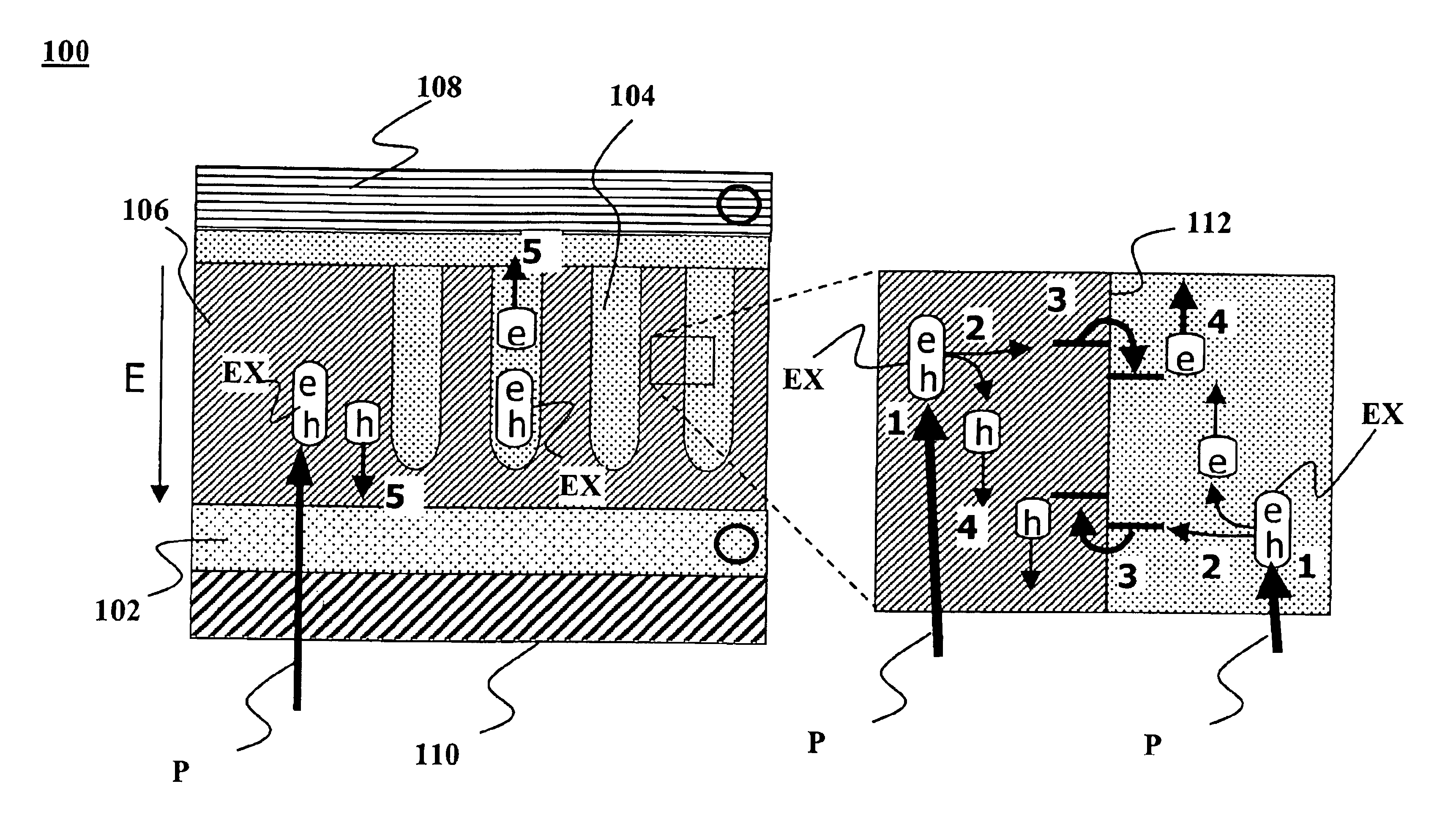
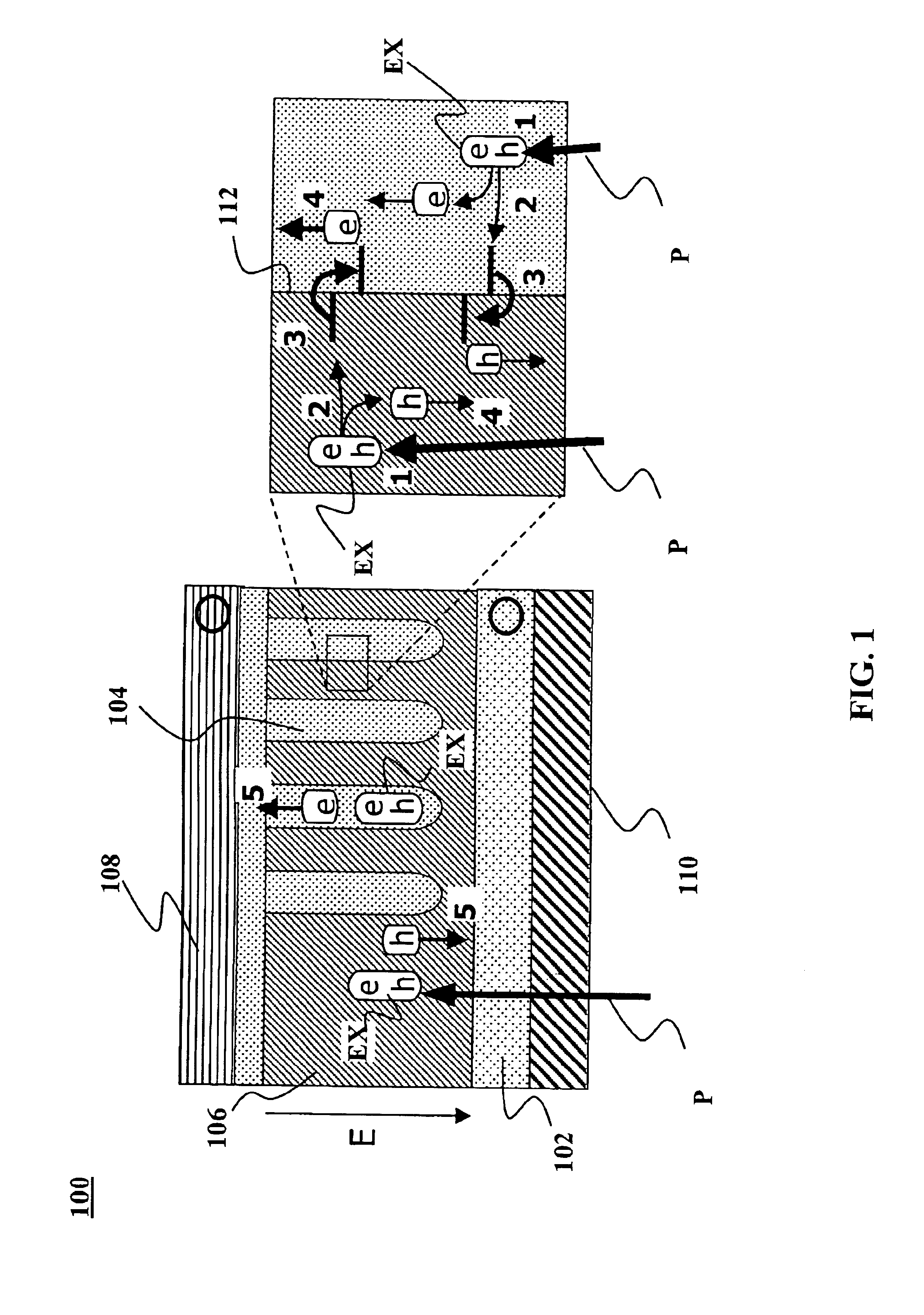
In an example of an embodiment of the present invention, arrays of nanoscale structures of conducting or semiconducting materials and conducting or semiconducting polymeric materials are used in an architecture for a highly efficient solar cell device. Other embodiments of the present invention are directed to solar cells and methods for the manufacture thereof, and more particularly, to solar cells comprising oriented nanoscale arrays of nanostructures in a matrix of conducting or semiconducting polymeric materials, where the nanostructures have ...


PUM

PropertyMeasurementUnit
distancesaaaaaaaaaa
distancesaaaaaaaaaa
distancesaaaaaaaaaa

Abstract

Nano-architected/assembled solar cells and methods for their manufacture are disclosed. The solar cells comprise oriented arrays of nanostructures wherein two or more different materials are regularly arrayed and wherein the presence of two different materials alternates. The two or more materials have different electron affinities. The two materials may be in the form of matrixed arrays of nanostructures. The presence of the two different materials may alternate within distances of between about 1 nm and about 100 nm. An orientation can be imposed on the array, e.g. through solution deposition surfactant templation or other methods.

Description

FIELD OF THE INVENTIONThis invention comprises solar cell devices and methods for their production, and more specifically to nano-architected / assembled solar cells.BACKGROUND OF THE INVENTIONIn the prior art, organic and hybrid solar cells have been fabricated with a polychromatic efficiency of 2% and a peak monochromatic efficiency of 7% (Huynh et al., “Hybrid NanoRod-Polymer Solar Cells”, Science 295, 2425-2427 (2002); Schmidt-Mende et al., “Self-Organized Discotic Liquid Crystals for High-Efficiency Organic Photovoltaics”, Science 293, 1119-1122 (2002)). In these solar cell devices, the device architecture is not adequate for that needed for a higher-efficiency device. These devices are limited by the extent to which excitons can be harvested to perform useful work. This is due to three different factors:First, the nanostructure within the active layer of the solar cells made by other groups were quasi-randomly arranged within a medium of conducting or semiconducting polymer, and...

Claims


Application Information

Patent Timeline
Patent Type & Authority Patents(United States)
IPC IPC(8): C08L65/00C08G75/00C08G75/12H01L21/00H01L35/12H01L31/042H01L31/0352H01L31/0248H01L31/0256H01L31/06H01L31/00H01L35/24H01L51/00H01L51/30H01L51/05H01G9/20H01L51/42H02J
CPCB82Y10/00H01L51/0012H01L51/422H01L51/4253H01L51/426B82Y30/00H01G9/2031H01L51/0035H01L51/0036Y02E10/549H01L51/005Y02E10/52Y10S977/948H01L51/0046Y02P70/50H10K71/191H10K85/111H10K85/113H10K85/211H10K85/60H10K30/15H10K30/30H10K30/35
Inventor SAGER, BRIAN M.ROSCHEISEN, MARTIN R.
Owner AERIS CAPITAL SUSTAINABLE IP
Why Eureka
Try Eureka