Self-assembled nanobump array stuctures and a method to fabricate such structures

a self-assembling, nano-bump array technology, applied in the direction of prosthesis, magnetic bodies, instruments, etc., can solve the problems of systematic atomic level characterization, technological barriers to fabricating functional device structures, and development of a controllable synthesis technology for making nano-sized structures

Inactive Publication Date: 2005-02-08
WAYNE STATE UNIV
View PDF31 Cites 33 Cited by
  • Summary
  • Abstract
  • Description
  • Claims
  • Application Information

AI Technical Summary

Problems solved by technology

It is believed that technological barriers may exist for fabricating functional device structures with characteristic dimensions below 1 μm.
These barriers may include problems in synthesizing the nano-sized structures in a sufficiently small dimension, in a specific pattern, or in a uniform size and spacing distribution.
Another difficulty in developing a controllable synthesis technology for making nano-sized structures may be attributed to the lack of systematic atomic level characterizations at various stages of the process.
Additionally, the inability to obtain localized topographic, chemical, magnetic, and electronic information may further limit the realization of specific nanostructure characteristics.
Such single crystal surface studies, however, merely represent the exposure of one crystal orientation, which foregoes potential opportunities offered by cluster-size effects.
Such efforts may,

Method used


Image

  • Self-assembled nanobump array stuctures and a method to fabricate such structures
  • Self-assembled nanobump array stuctures and a method to fabricate such structures
  • Self-assembled nanobump array stuctures and a method to fabricate such structures

Examples


Embodiment Construction

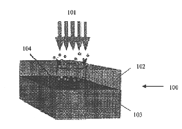
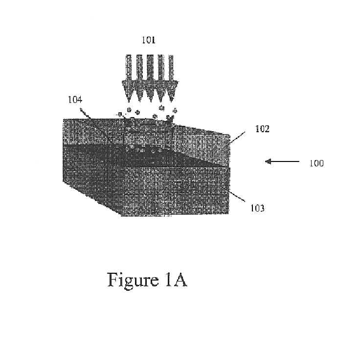
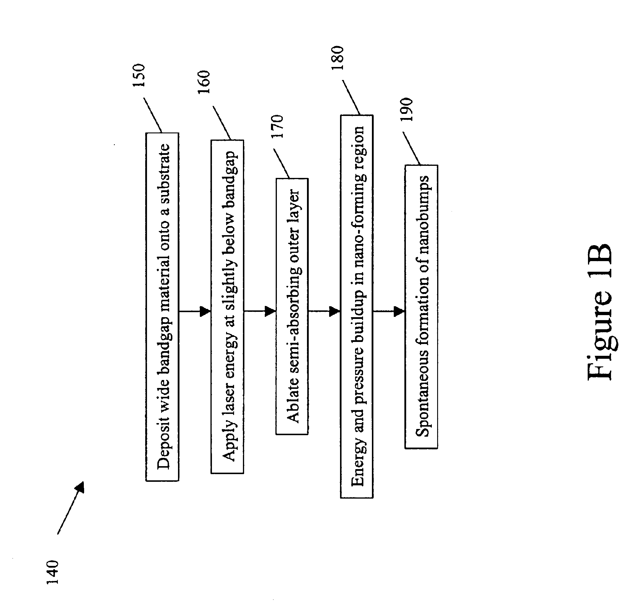
The exemplary embodiments and / or exemplary methods of the present invention involve using a laser to irradiate composite layered structures to induce a spontaneous formation of nano-sized array structures in a controllable manner. The micro and / or nano-sized array structures (that is, the “nanobumps”) arise from the layered composites during ablation of a semi-absorbing outer layer. The laser includes, for example, an Excimer laser. Furthermore, the exemplary method may involve depositing a wide bandgap semiconductor material upon one or more underlying substrate layers to form the composite-layered structure. The laser energy is then applied to the composite layered structure using an Excimer laser at a predefined wavelength. If the applied laser energy is slightly below the bandgap of the deposited wide bandgap semiconductor material, a partial or semi-absorption of the laser energy may occur in the deposited material. The semi-absorbing wide bandgap semiconductor material compris...


PUM


Abstract

A self-assembled nanobump array structure including a semi-absorbing outer layer provided on at least one nanobump-forming substrate layer, the semi-absorbing outer layer configured to ablate slowly to allow an applied laser energy to be transmitted to the at least one nanobump-forming substrate layer, in which the self-assembled nanobump array structure is formed by an energy and a pressure buildup occurring in the at least one nanobump-forming substrate layer.

Description

FIELD OF THE INVENTIONThe present invention relates to laser assisted spontaneously formed nanobump array structures and a method for making such structures.BACKGROUND INFORMATIONIt is believed that technological barriers may exist for fabricating functional device structures with characteristic dimensions below 1 μm. These barriers may include problems in synthesizing the nano-sized structures in a sufficiently small dimension, in a specific pattern, or in a uniform size and spacing distribution. Furthermore, such nano-sized structures may require direct fabrication into microsystems to allow proper functioning. For example, a neural stimulatory microsystem may require fairly uniform nano-sized electrode arrays for use in focally stimulating neural tissue to treat blindness, as well as Parkinson disease, Huntington disease, and other neurological disorders. In one particular application, focal stimulation may require electrodes or groups of electrodes on the order of 100 nanometers...

Claims


Application Information

Patent Timeline
IPC IPC(8): H01L21/02H01L21/44H01L23/48B23K35/36G01N29/02G01N29/24G01N29/34G11B5/855H01F1/00H01L21/20H01L21/205H01L31/00H01L51/00H01L51/10
CPCB23K35/36B82Y10/00G01N29/022G01N29/2418G01N29/2437G01N29/34G11B5/855A61F9/08Y10S977/816A61F2002/3084A61F2002/3097B82Y25/00G01N2291/0255G01N2291/0256G01N2291/0422G01N2291/0423H01F1/009H01L21/0237H01L21/02378H01L21/0242H01L21/02491H01L21/0254H01L21/0259H01L21/02631H01L51/0595H01L51/102Y10S977/889A61F2002/30701A61F2002/307H10K10/82H10K10/701
Inventor AUNER, GREGORY W.NAIK, RATNANG, SIMONABRAMS, GARY W.MCCALLISTER, JAMES PATRICKIEZZI, RAYMOND
Owner WAYNE STATE UNIV
Why Eureka
Try Eureka