
NANO patterning method and methods for fabricating surface plasmon color filter and liquid crystal display device using the same

a color filter and liquid crystal display technology, applied in the field of nano patterning methods, can solve the problems of difficult to have a transmittance rate more than 30%, complicated process for related art color filters, and increased power consumption of backlights, so as to enhance the aperture ratio and the transmittance rate of the lc panel. , the effect of enhancing the transmittance ra

Active Publication Date: 2011-11-03
LG DISPLAY CO LTD
View PDF3 Cites 33 Cited by
  • Summary
  • Abstract
  • Description
  • Claims
  • Application Information

AI Technical Summary

Benefits of technology

[0022]Therefore, an aspect of the detailed description is to provide a method for fabricating a surface plasmon color filter capable of enhancing an aperture ratio and a transmittance rate of an LC panel, by forming a color filter having an enhanced transmittance rate by using a surface plasmon instead of using the general dyes or pigments, and a method for fabricating a liquid crystal display (LCD) device having the same.
[0024]Still another aspect of the detailed description is to provide a nano patterning method capable of simplifying processes, reducing fabrication costs, and being applied onto a large area of a substrate, and methods for fabricating a surface plasmon color filter and an LCD device using the same.
[0030]According to the nano patterning method of the present invention, two-dimensional nano holes arranged in a hexagonal lattice and having a period may be fabricated by using the stamp which provides a partial electrification region, and the template, the thiol-terminated nanospheres which can undergo a self assembly process. This may allow a surface plasmon color filter and an LCD device to be fabricated through simplified processes and with low costs.
[0031]According to the methods for fabricating a surface plasmon color filter and an LCD device having the same, a color filter having a simplified structure may be formed by using a surface plasmon phenomenon, instead of using the general dyes or pigments. This may simplify fabrication processes, and reduce fabrication costs.
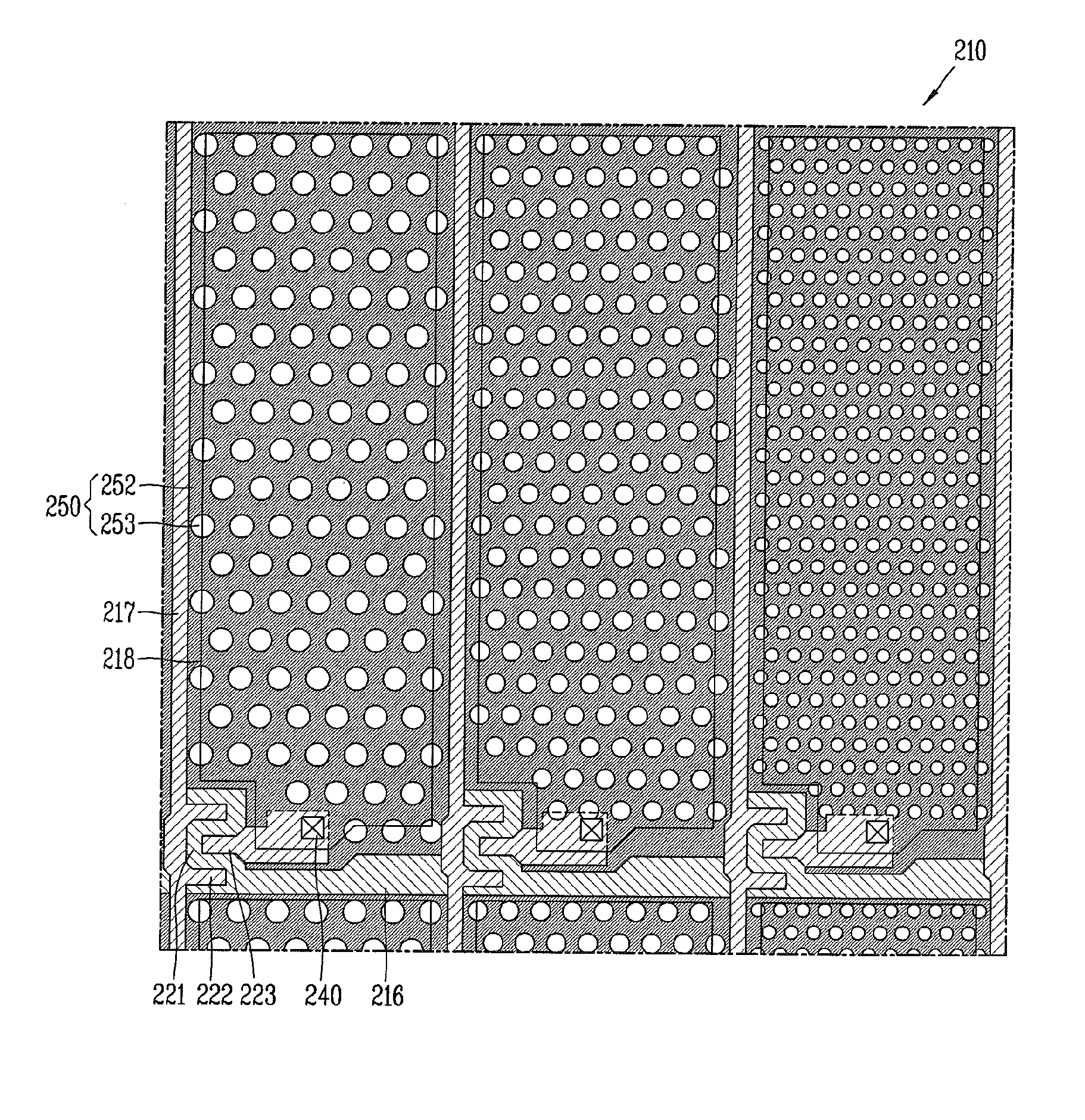
[0032]According to the methods for fabricating a surface Plasmon color filter and an LCD device having the same, a hexagonal lattice structure may be adopted such that six nearest holes are positioned near one hole of the transmissive pattern. This may enhance an aperture ratio more than in a square lattice structure by 15% or more. As a result, a full color filter which provides excellent monochromaticity and transmittance rate may be implemented. A size of the holes of the surface plasmon color filter may be controlled by a diameter of the nanospheres, and a lattice period of the holes may be determined by controlling a length of the thiol-terminated polymers.

Problems solved by technology

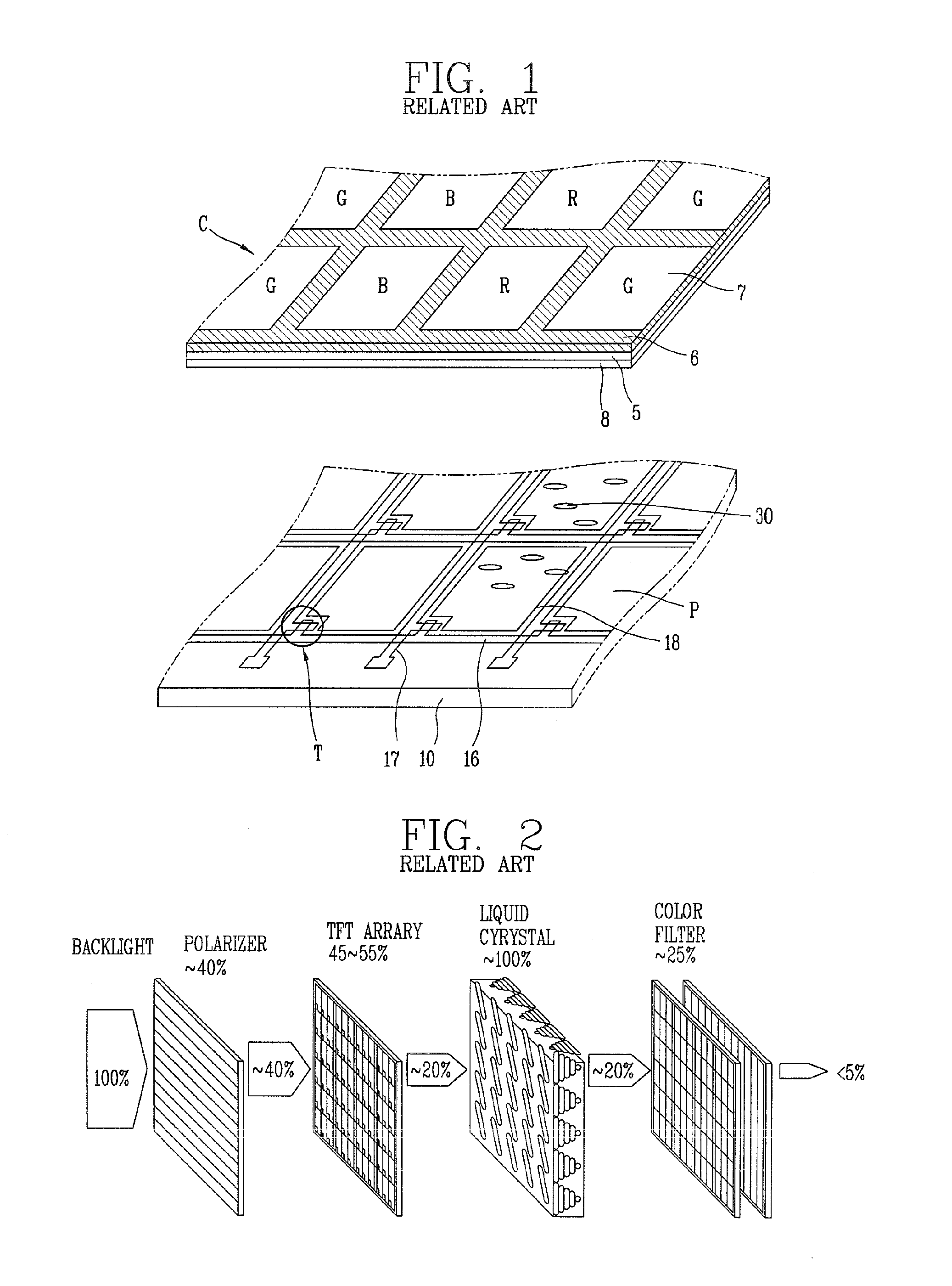
Accordingly, it is difficult to have a transmittance rate more than 30%.
Due to this low transmittance rate of the LC panel, power consumption by a backlight is increased.
The related art color filter is fabricated with complicated processes since it repeatedly undergoes color resist coating, exposure to light, development and curing processes according to each color.
Firstly, devices or processes require high costs, and include complicated processes.
Accordingly, it takes a long time to perform the entire processes.
Furthermore, it is limited to develop polymers used as a photoresist under a UV wavelength and to develop equipment.
Especially, the electron beam lithography is an expensive processing technology using a sequential writing method which requires a long processing time.
Furthermore, high costs are required when fabricating, by an electron beam lithography, a stamp having a large area of a high-density nano pattern.
Accordingly, it is expensive to fabricate the master mould.
Furthermore, since a sequential repeat printing method is adopted, the productivity per hour may be degraded as a pattern area is increased.

Method used


Image

  • NANO patterning method and methods for fabricating surface plasmon color filter and liquid crystal display device using the same
  • NANO patterning method and methods for fabricating surface plasmon color filter and liquid crystal display device using the same
  • NANO patterning method and methods for fabricating surface plasmon color filter and liquid crystal display device using the same

Examples


first embodiment

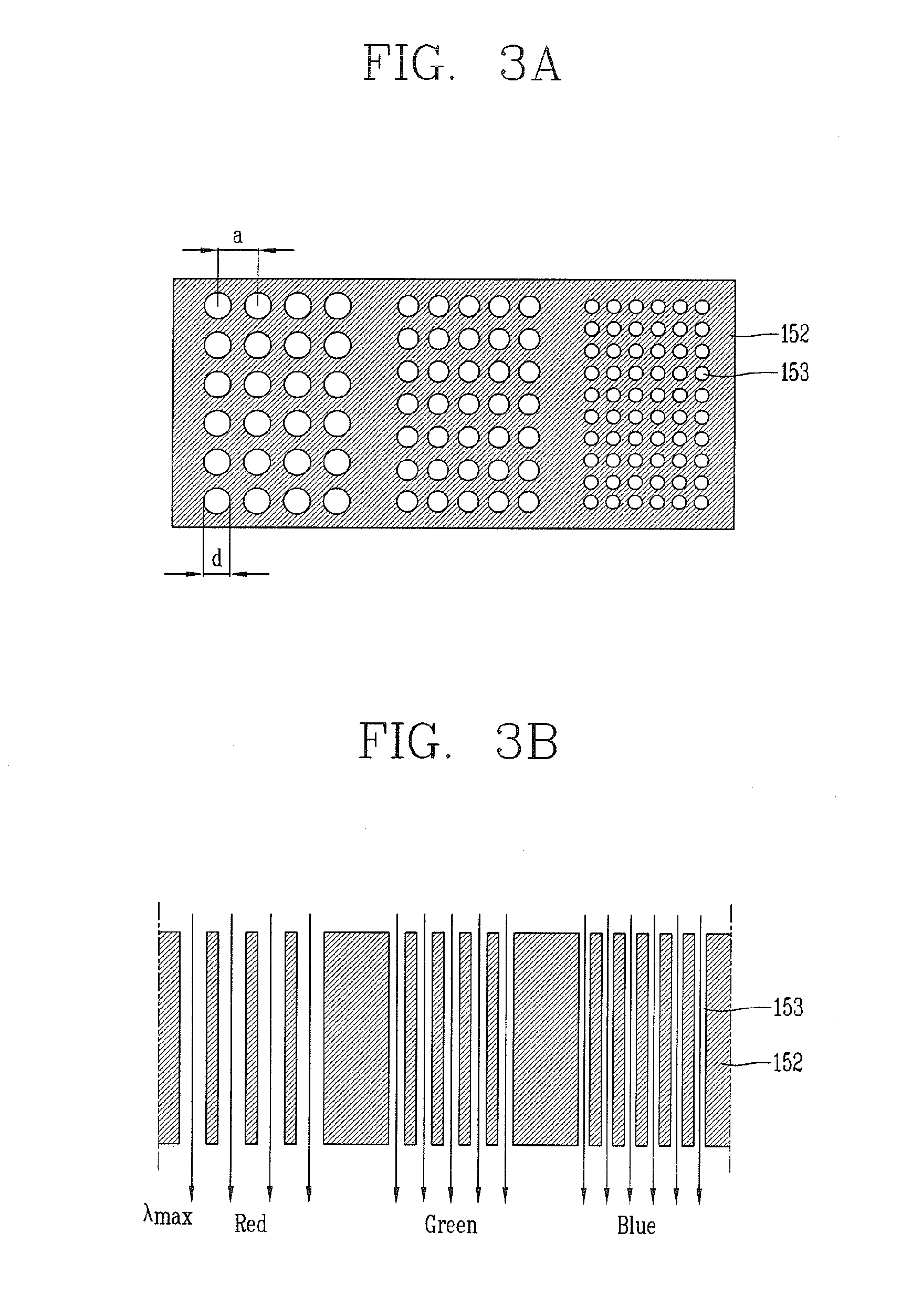
[0055]FIGS. 3A and 3B are respectively planar and sectional views schematically showing a structure of a color filter fabricated by using a surface plasmon phenomenon according to the present invention.

[0056]Referring to FIG. 3, a transmissive pattern 153 consisting of a plurality of sub-wavelength holes having a predetermined period (L) is formed in a metallic film 152. An electric field of incident light having both a wavelength of near infrared light and a wavelength of visible light is coupled to a plasmon. Accordingly, only light of specific wavelengths is transmitted, and light of other wavelengths is reflected, thereby obtaining RGB colors.

[0057]For instance, if a sub-wavelength hole pattern having a predetermined period (L) is formed on a silver film, RGB light of specific wavelengths selected according to a size (d) and a period (L) of holes is transmitted, thereby implementing RGB colors. A greater amount of light than a hole area may be transmitted by absorbing light near...

second embodiment

[0079]FIGS. 6A and 6B are respectively a planar view and a sectional view, which schematically show a structure of a color filter fabricated by a surface plasmon phenomenon according to the present invention.

[0080]Referring to FIG. 6, the color filter according to the second embodiment of the present invention has a hexagonal lattice structure in which the holes of the transmissive pattern 253 are periodically arranged. Once the transmissive pattern 253 consisting of a plurality of sub-wavelength holes having a predetermined period (a) is formed in the metallic film 252, an electric field of incident light having both a wavelength of near infrared light and a wavelength of visible light is coupled to a plasmon. Accordingly, only light of specific wavelengths is transmitted, and light of other wavelengths is reflected, thereby obtaining RGB colors.

[0081]If light is incident from a lower side of the color filter substrate, only light of a specific wavelength determined by a lattice pe...


PUM

PropertyMeasurementUnit
Lengthaaaaaaaaaa
Diameteraaaaaaaaaa
Structureaaaaaaaaaa

Abstract

Disclosed are a nano patterning method for fabricating a surface plasmon color filter having a transmissive pattern which selectively transmits light of specific wavelengths, and methods for fabricating a surface plasmon color filter and a liquid crystal display (LCD) device using the same. Used are a stamp which provides a partial electrification region, and a template, thiol-terminated nanospheres which can be self-assembled, thereby fabricating nano holes having a two-dimensional period and arranged in a hexagonal lattice. This may be applied onto a large area of a substrate, and may implement simplified processes and reduced fabrication costs.

Description

CROSS-REFERENCE TO RELATED APPLICATION[0001]Pursuant to 35 U.S.C. §119(a), this application claims the benefit of earlier filing date and right of priority to Korean Application No. 10-2010-0040267, filed on Apr. 29, 2010, the contents of which is incorporated by reference herein in its entirety.1. FIELD OF THE INVENTION[0002]This specification relates to a nano patterning method using self assembly characteristics, and methods for fabricating a surface plasmon color filter and a liquid crystal display (LCD) device using the same, and particularly, to a nano patterning method for fabricating a surface plasmon color filter having a transmissive pattern which selectively transmits light of specific wavelengths, and methods for fabricating a surface plasmon color filter and a liquid crystal display (LCD) device using the same.2. DESCRIPTION OF THE RELATED ART[0003]As concerns about an information displays and demands for portable information media are increased, research and commercial...

Claims


Application Information

Patent Timeline
IPC IPC(8): H01J9/24C23F1/04
CPCG02B5/201G02F1/133514G02F1/133516G02F2001/136222B82Y40/00G03F7/0002G03F7/0007G03F7/165B82Y10/00G02F2203/10G02F1/136222
Inventor YOON, MIN-SUNG
Owner LG DISPLAY CO LTD
Learn More