

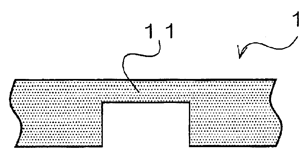
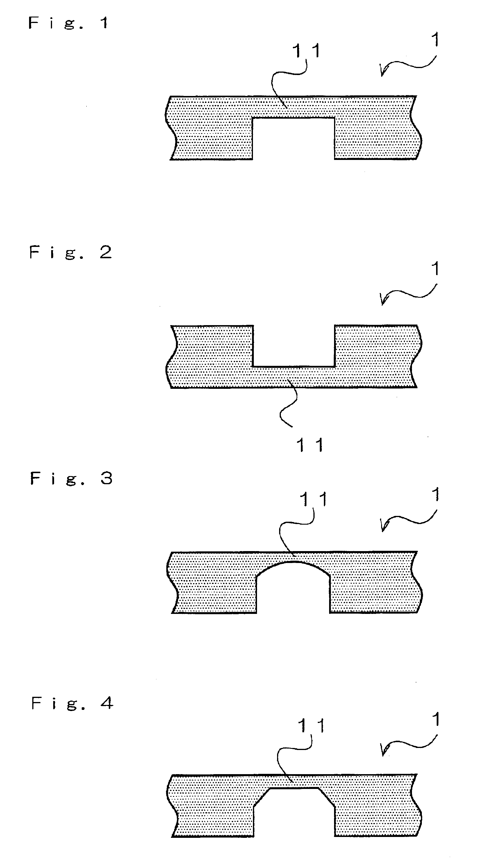
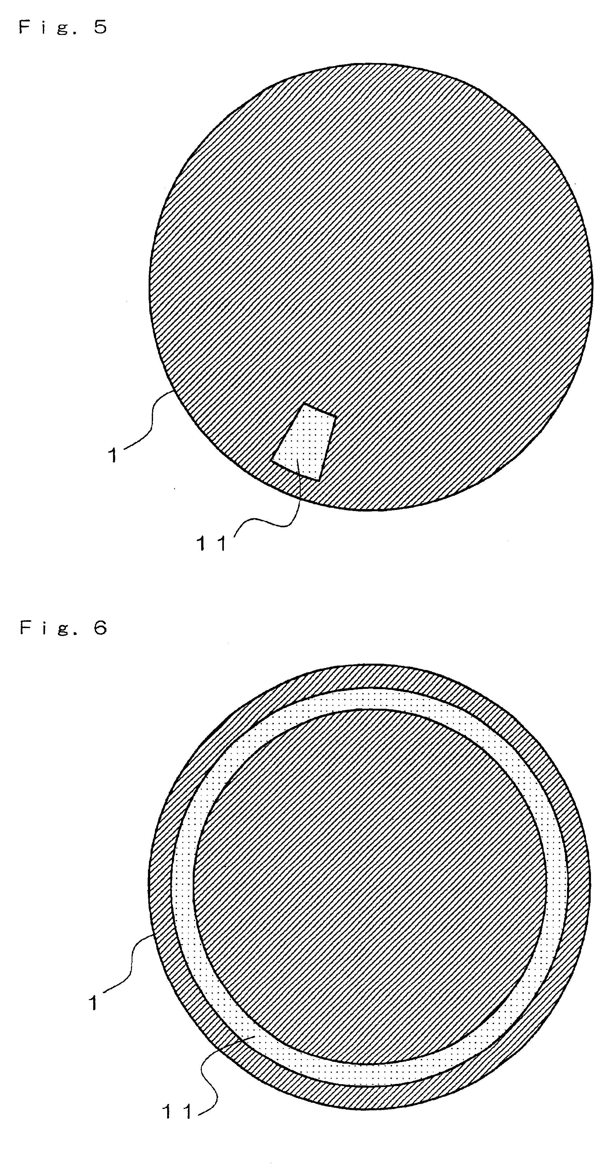
Polishing pad for semiconductor wafer and laminated body for polishing of semiconductor wafer equipped with the same as well as method for polishing of semiconductor wafer
a technology for polishing pads and semiconductor wafers, which is applied in the direction of flexible wheels, manufacturing tools, lapping machines, etc., can solve the problems of inability to achieve inefficient to obtain all polishing times in a variety of different polishings, and inability to achieve essential ability
- Summary
- Abstract
- Description
- Claims
- Application Information
AI Technical Summary
Benefits of technology
Problems solved by technology
Method used
Image

Examples
example 1
[1] Preparation of a Polishing Pad
80% by volume of 1,2-polybutadiene (trade name “JSR RB830” manufactured by JSR Corp.) which becomes a water-insoluble matrix material by crosslinking later, and 20% by volume of β-cyclodextrin (trade name “Dexypearl β-100” manufactured by Yokohamakokusaibiokenkyusho Co. Ltd.) were kneaded with a kneader heated to 120° C. Thereafter, 0.2 part by mass of dicumyl peroxide (trade name “Percumyl D” manufactured by NOF Corp.) was added to a total of 100 parts by mass of total of 1,2-polybutadiene and β-cyclodextrin, which was further kneaded, reacted to crosslink at 170° C. for 20 minutes in a press mold, and molded to obtain a disc-like polishing pad having a diameter of 60 cm and a thickness of 2 mm.
[2] Measurement of the Transmittance
The transmittance of the resulting polishing pad at a wavelength ranges between 400 and 800 nm was measured at five different points on the polishing pad using a UV absorbance measuring device (Model “U-2010” manufactured ...
example 2
Using a polishing pad composed of commercially available polyurethane foam having no light transmitting properties (trade name “IC1000” manufactured by Rodel Nitta), polishing was performed under the same conditions as those of Example 1, and a removal rate was 950 Å / min. A circular through hole having a diameter of 20 mm was provided on this polishing pad, and a light transmitting part having the same constituent as that of the polishing pad in the above-mentioned Example 1 was fitted therein. Polishing was performed under the same conditions as those of Example 1 using this new polishing pad, and a removal rate was 950 Å / min.
As a result, even when, a light transmitting part molded in a prescribed size is fitted in a through hole provided on a part of a polishing pad composed of polyurethane foam having no light transmitting properties to obtain a polishing pad, which is used to perform polishing, it can be seen that the polishing performance of a polishing pad composed of polyuret...
PUM
| Property | Measurement | Unit |
|---|---|---|
| thickness | aaaaa | aaaaa |
| integrated transmittance | aaaaa | aaaaa |
| thickness | aaaaa | aaaaa |
Abstract
Description
Claims
Application Information