

Method and device for making substrates
a substrate and substrate technology, applied in the direction of polycrystalline material growth, crystal growth process, after-treatment details, etc., can solve the problem of not producing substrates with satisfactory dimensions for some applications, and achieve the effect of preventing problems associated with its fragility or deformability
- Summary
- Abstract
- Description
- Claims
- Application Information
AI Technical Summary
Benefits of technology
Problems solved by technology
Method used
Image

Examples
example 1
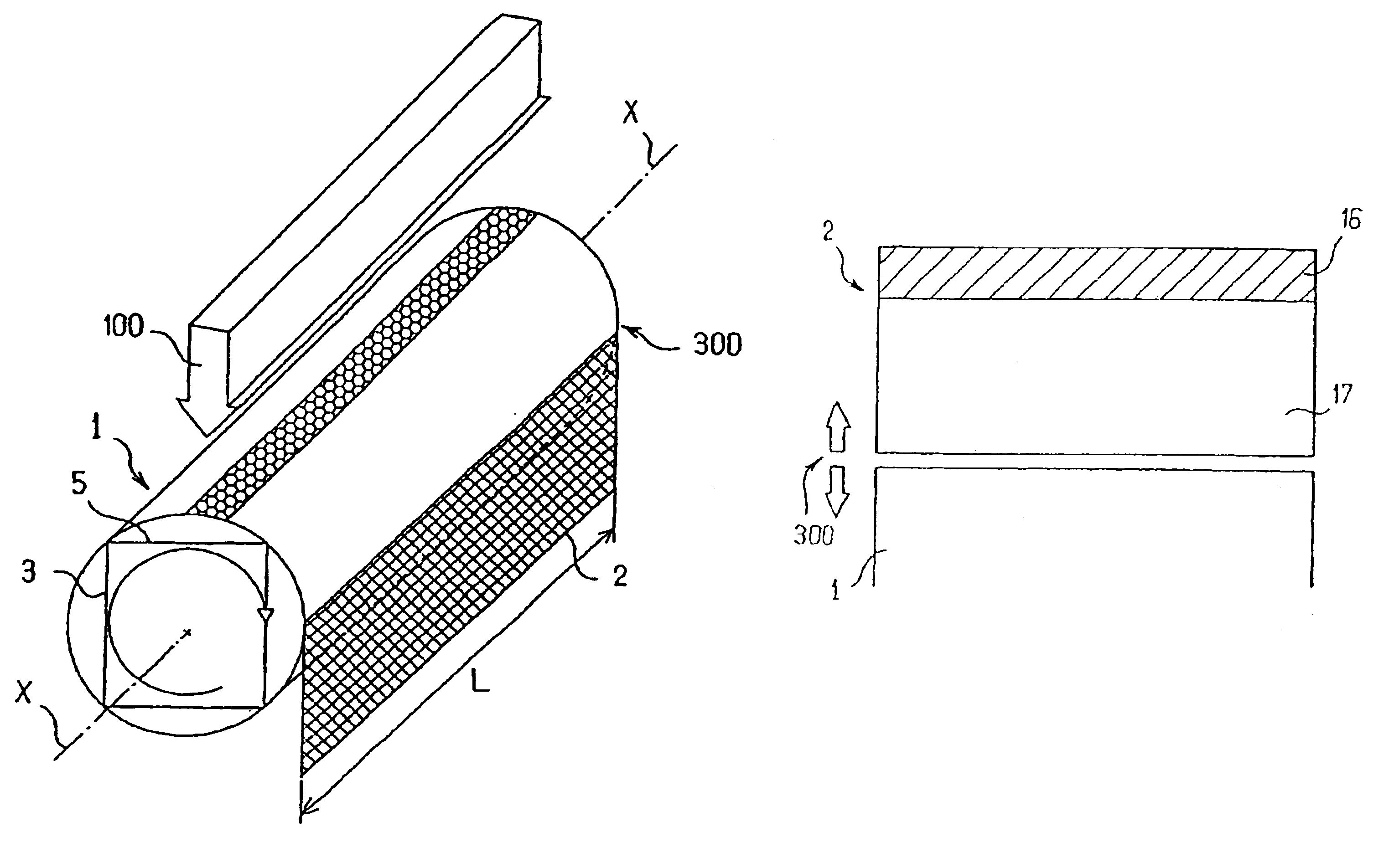
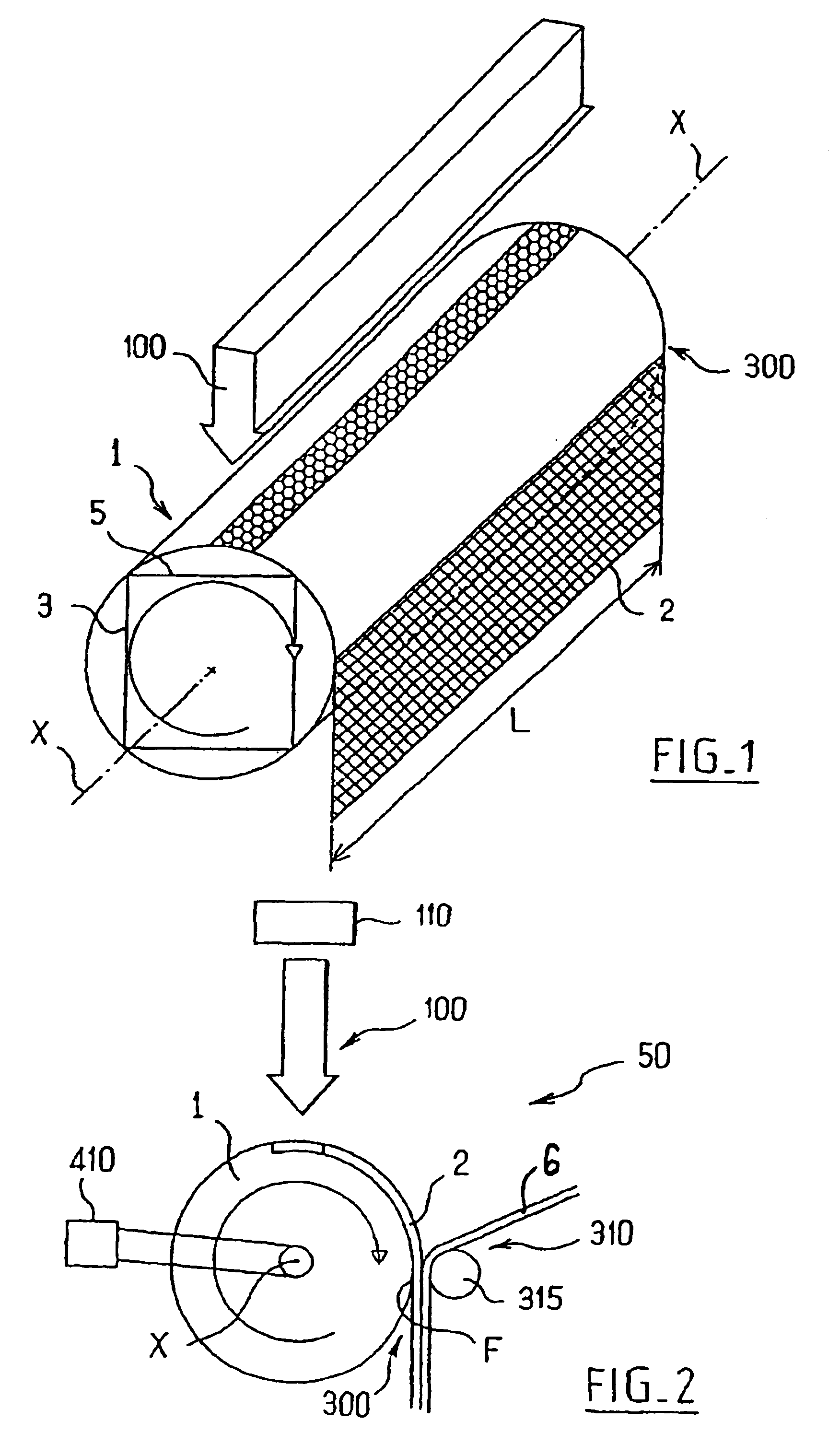
[0068]In the first example, shown in FIG. 1, the method according to the invention includes an operation 100 of implanting atomic species and a detachment operation 300.
[0069]In this example, the atomic species are H− ions. They are implanted with a high energy. The beam made up of these ions is elongate in the longitudinal direction of the ingot. To obtain a 10 μm thick layer 2 of silicon the H− ions are accelerated with an energy of 725 keV. The amount of H− ions implanted is 1.21×10¹⁷ / cm2.
[0070]The implantation operation 100 is carried out by sweeping a beam of accelerated atomic species over the surface of the ingot 1, over the whole of its length, matching the rotation speed of the ingot 1 to the width of the beam and to the sweeping rate to obtain the appropriate dose.
[0071]The implantation depth Rp varies according to the crystallographic orientation of the implanted surface relative to the incident beam of atomic species. In applications in which variations in the thickness ...
example 2
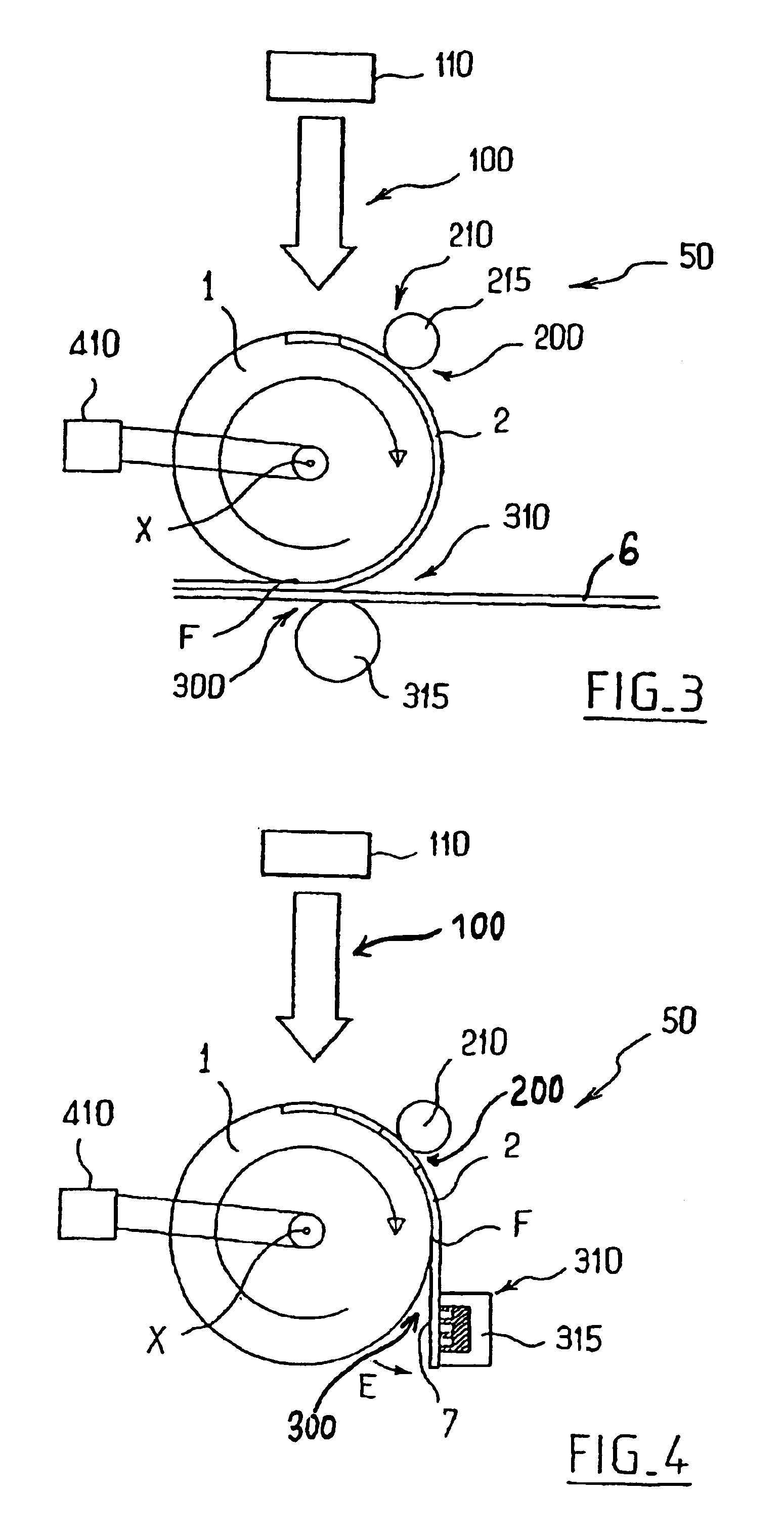
[0079]A second example of implementation of the method according to the invention, shown in FIG. 3, includes an implantation operation 100, a heating operation 200 and a detachment operation 300.
[0080]The species implanted are advantageously hydrogen ions. Hydrogen ions are implanted with an energy of the order of 700 keV and a dose of the order of 1017 / cm2.
[0081]With the ingot 1 rotating continuously about its axis X—X in the device 50, the area of the surface of the ingot 1 bombarded by the atomic species during the implantation operation 100 moves towards a heating area.
[0082]The heating operation 200 is carried out after the implantation operation 100 by heating means 210. The heating operation 200 assists detaching the layer 2 between the surface and the detachment depth from the remainder of the ingot 1. The heating operation 200 enables the doses of atomic species implanted to be reduced relative to the dose referred to in example 1.
[0083]The heating means 210 consist of a he...
example 3
[0085]A third example of implementation of a device 50 for implementing a method according to the invention, shown in FIG. 4, includes an implantation operation 100 and a heating operation 200, like those of example 2, plus a detachment operation 300 performed with the aid of holding means 310. The holding means 310 can employ a pressure difference, an electrostatic force, a reversible adhesion force (by application of a low-tack adhesive), etc.
[0086]If the holding means 310 are of the suction type, they advantageously comprise a bar 315 with its length parallel to the axis X—X of the ingot 1. The bar 315 is hollow. The pressure inside the bar is reduced to hold the layer 2 reversibly by suction. Detachment of the layer 2 from the remainder of the ingot 1 is encouraged by the heating operation 200.
[0087]To begin peeling the layer 2 off the ingot 1, the holding means 310 are applied to the first area of the ingot 1 that has been subjected to the implantation operation 100 and the hea...
PUM
| Property | Measurement | Unit |
|---|---|---|
| diameter | aaaaa | aaaaa |
| diameter | aaaaa | aaaaa |
| lengths | aaaaa | aaaaa |
Abstract
Description
Claims
Application Information