Semiconductor radiation imaging device including threshold circuitry

a radiation imaging and semiconductor technology, applied in the field of electromagnetic resonance imaging devices, can solve the problems of spoiling image resolution and contrast, light diffusion worsening resolution and contrast, and ccds having an additional limitation of low efficiency

Inactive Publication Date: 2005-02-15
SIEMENS HEALTHCARE GMBH
View PDF8 Cites 29 Cited by
  • Summary
  • Abstract
  • Description
  • Claims
  • Application Information

AI Technical Summary

Benefits of technology

Accordingly, an object of the invention is to provide an imaging device based on a different approach which enables the problems of the prior art to be mitigated and / or solved.

Problems solved by technology

During this process no further charge can be accumulated as it would destroy the information of the charge content per pixel and consequently it would spoil image resolution and contrast.
When used for detecting incident radiation as well as for reading the signals, CCDs have an additional limitation of low efficiency.
However light diffusion worsens resolution and contrast.
As a result of the above the CCD is a device with two substantial limitations:
1) Compromised dynamic range. Typically a CCD can accumulate 100,000-700,000 electrons. The reason for the limited dynamic range is that the potential well fills up due to the dark current within the Si volume, the electrode gate surface under which the charge is accumulated is at best ⅓ of the total pixel area (thus not utilizing the total charge storage capacity of the pixel) and the oxide layer thickness upon which the storage capacity also depends has to be thick to stand the abrupt voltage pulses needed for the readout (note: the thicker the oxide layer, the less charge can be stored in the potential well).
2) Large inactive time. The inactive time needed for the readout is considerable. In many cases this inhibits CCDs from being used for fast dynamic multi-frame image accumulation.
However, they cannot cope with high intensity applications because the readout electronics will overflow or counting ability saturates thus destroying the image contrast.
In some of these devices simultaneously incident rays cause ambiguous and ‘ghost’ hits that cannot be resolved and worsen the resolution.
Although these devices directly detect the incident radiation, they have limitations due to an operation based on a single pulse counting mode and imaging based on the counting of discrete points.
In particular CCDs enable charge from successive hits to be accumulated, but only to the limited extent possible within a potential well inside the Si substrate, which substantially limits the dynamic range.
Thus, until all pixels are read out as a time train sequence, a CCD cannot accumulate a new image frame since additional incoming radiation and / or light would not be recorded in one to one correspondence with a pixel position during the readout process.
Therefore limited dynamic range and large inactive time during imaging are the two major CCD limitations.
These devices operate on the single pulse counting mode and suffer from saturation problems at high counting rates.
Such conventional single hit counting devices have a very small dynamic range.

Method used


Image

  • Semiconductor radiation imaging device including threshold circuitry
  • Semiconductor radiation imaging device including threshold circuitry
  • Semiconductor radiation imaging device including threshold circuitry

Examples


Embodiment Construction

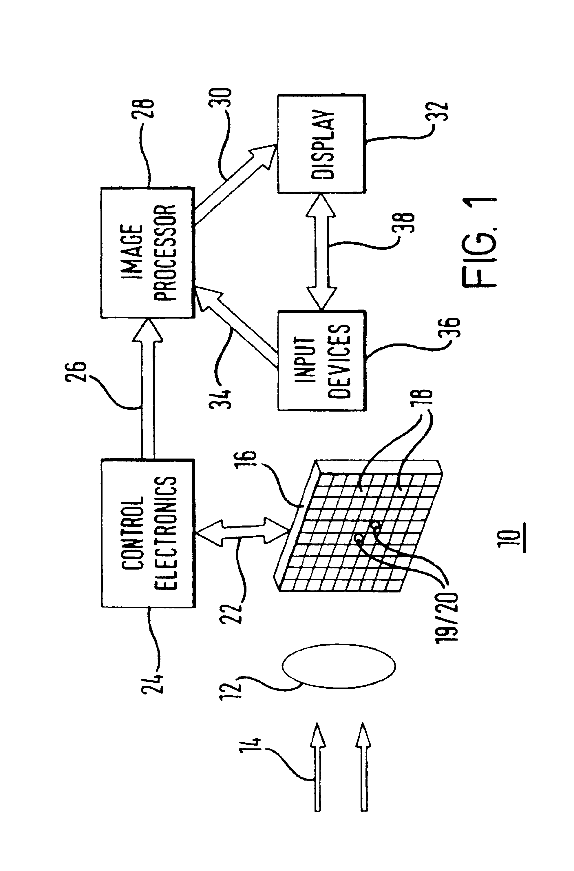
FIG. 1 is a schematic representation of an example of an application for an imaging system 10 including an embodiment of an imaging device in accordance with the invention.

This application relates to radiation imaging of an object 12 subjected to radiation 14. The radiation may, for example, be X-ray radiation and the object 12 may, for example be a part of a human body.

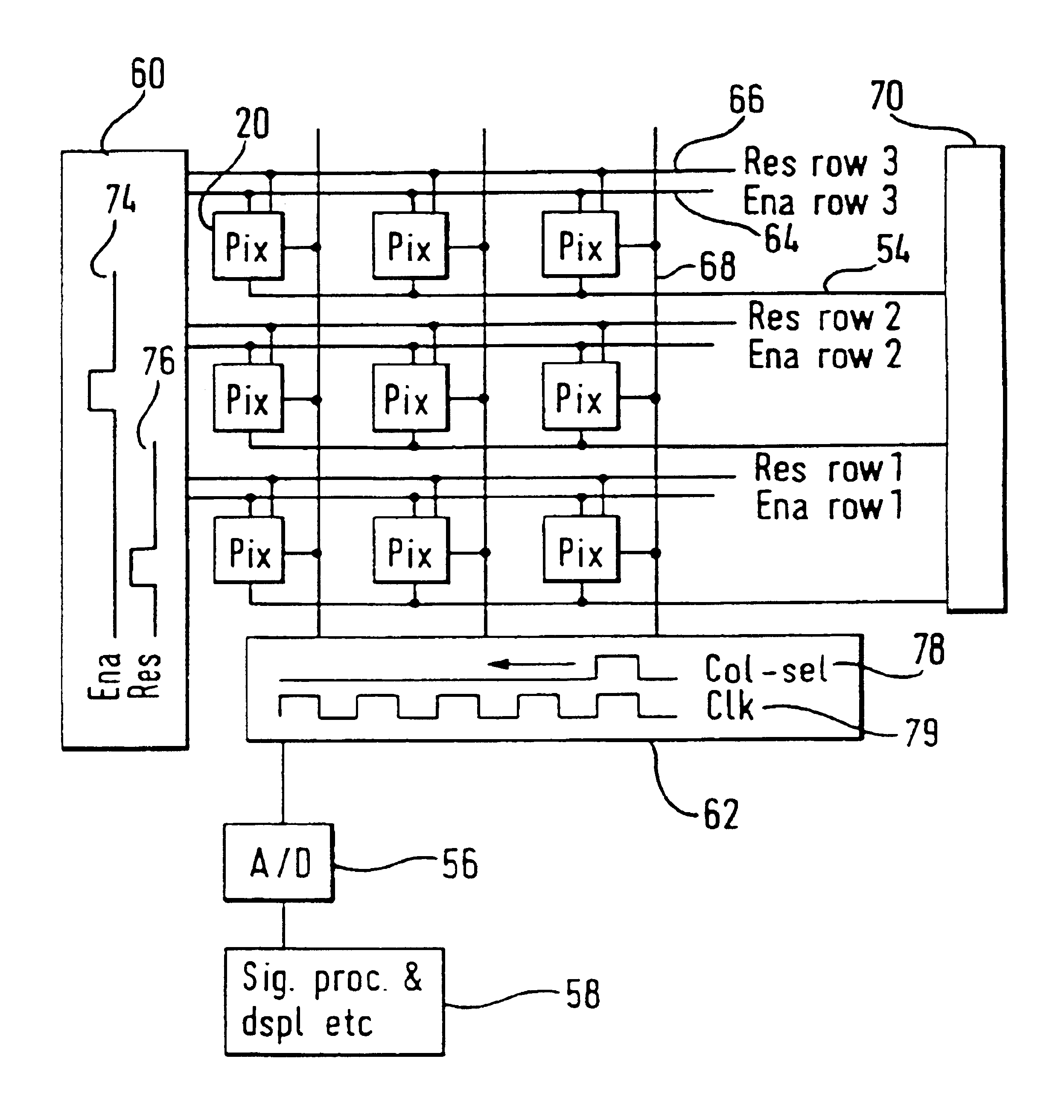
The imaging device comprises an Active-pixel Semiconductor Imaging Device (ASID) 16 comprising a plurality of pixel cells 18. The imaging device detects directly high energy incident radiation such as X-rays, γ-rays, β-rays or α-rays and accumulates at each pixel cell, by means of a randomly accessible, active, dynamic pixel circuit on or adjacent to a corresponding pixel cell detector, values representative of the radiation incident at that pixel cell.

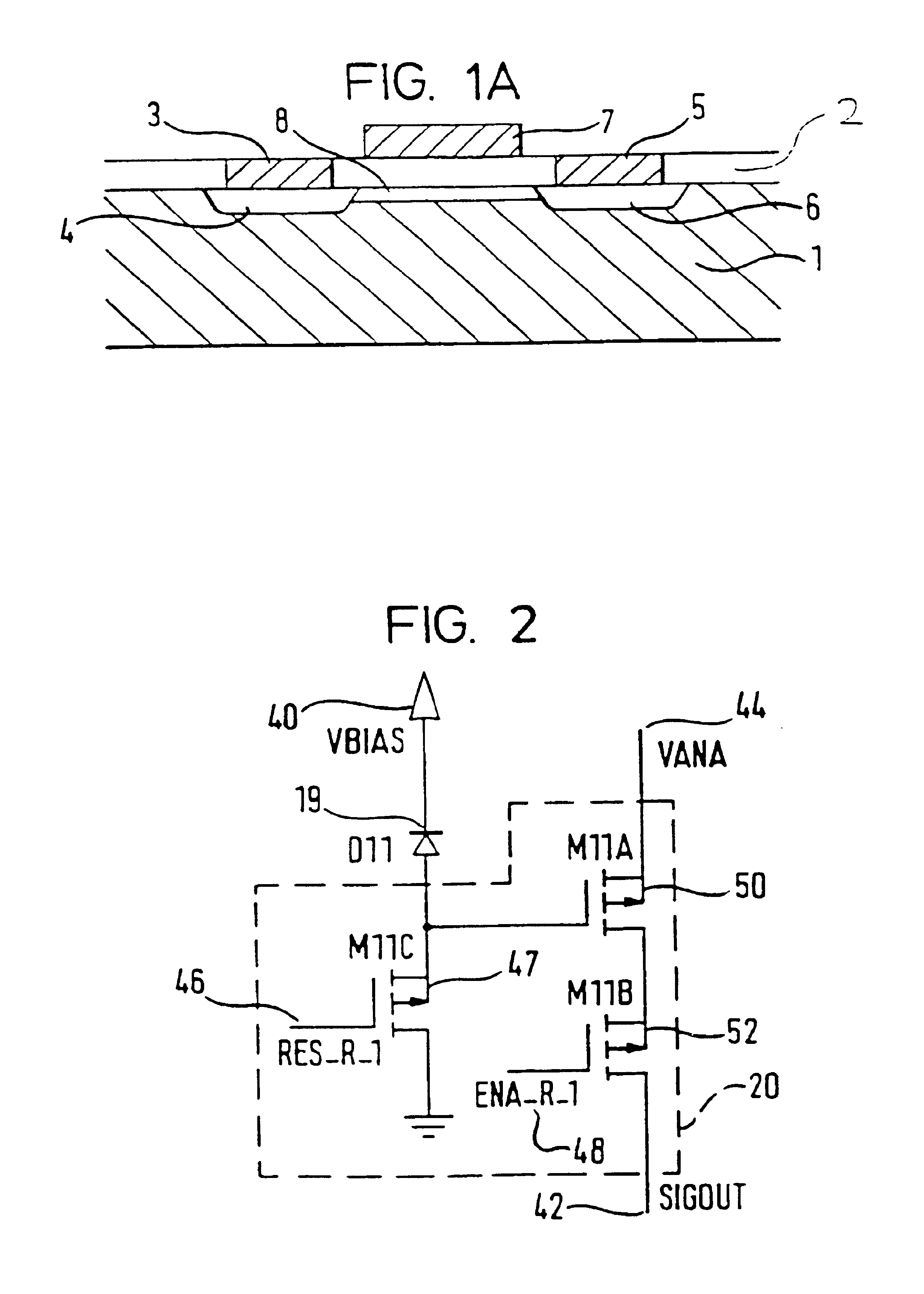
The ASID can be configured as a single semiconductor substrate (e.g., silicon) with each pixel cell comprising a pixel detector 19 and an active pixel circuit 20. Alte...


PUM


Abstract

A semiconductor radiation imaging device includes an array of pixel cells having an array of pixel detectors which directly generate charge in response to incident radiation and a corresponding array of individually-addressable pixel circuits. Each pixel circuit is associated with a respective pixel detector for accumulating charge directly resulting from radiation incident on the pixel detector and includes threshold circuitry and charge accumulation circuitry. The threshold circuitry is configured to discard radiation hits on the pixel detector outside a predetermined threshold range, and the charge accumulation circuit is configured to accumulate charge directly resulting from a plurality of successive radiation hits on the respective pixel detector within the predetermined threshold range.

Description

BACKGROUND OF THE INVENTION1. Field of the InventionThe invention relates to imaging devices, systems and methods, and in particular to a semiconductor pixel imaging device for use as an image sensor and to imaging systems and methods utilizing the pixel semiconductor imaging device.2. Description of the Prior ArtTwo basic types of semiconductor pixel devices are known in the prior art:1) Charge Coupled image sensors also known as Charge Coupled Devices (CCD) and2) Pulse Counting Semiconductor Pixel Devices.CCDs have been used for the past 15 years or so (see for example S. M Sze “Physics of Semiconductor Devices” 2nd Edition, 1981) as image sensors. Practically all CCDs available are made using silicon (Si) technology. The principle of operation of a CCD is based on the fact that when an appropriate voltage is applied via an electrode gate, the bulk Si volume becomes depleted of majority carriers (e.g. holes) and a region is created (depletion region) where electrons can be accumul...

Claims


Application Information

Patent Timeline
Patent Type & Authority Patents(United States)
IPC IPC(8): G01T1/00G01T1/29G01T1/24H01L27/148H01L27/146H04N3/15H04N5/32H04N5/321H04N5/325H04N5/335H01L27/14
CPCG01T1/2928G01T1/247H01L27/146H01L27/14601H01L27/14676H01L27/14831H04N3/1512H04N3/155H04N3/1568H04N3/1587H04N3/1593H04N5/32H04N5/325H04N5/335G01T1/2964H04N25/48H04N25/74H04N25/77H04N25/76
Inventor ORAVA, RISTO OLAVIPYYHTIA, JOUNI ILARISCHULMAN, TOM GUNNARSARAKINOS, MILTIADIS EVANGELOSSPARTIOTIS, KONSTANTINOS EVANGELOS
Owner SIEMENS HEALTHCARE GMBH
Why Eureka
Try Eureka