Line profile asymmetry measurement using scatterometry

a scatterometry and line profile technology, applied in the direction of semiconductor/solid-state device testing/measurement, instruments, photomechanical equipment, etc., can solve the problems of complex process for the fabrication of microelectronic devices, device integrity or functionality may also be compromised, and the device may not function at all

Inactive Publication Date: 2005-02-15
ONTO INNOVATION INC
View PDF39 Cites 181 Cited by
  • Summary
  • Abstract
  • Description
  • Claims
  • Application Information

AI Technical Summary

Problems solved by technology

The fabrication of a microelectronic device is a complicated procedure that uses a variety of equipment for the different process steps involved.
If errors occur during the processing this desired symmetry may be compromised, and as a result the device integrity or functionality may also be compromised.
If the asymmetry is quite severe the device may not function at all.
However, there is no disclosure of using such a technique to determine asymmetry.
The local presence of topography on a material being examined causes a perturbation of the probing radiation and hence a ‘blip’ in the intensity of the probing radiation.
U.S. Pat. No. 5,982,489 relates to depth measurement only and not line profile (so it is not possible to determine line profile asymmetry).
The hardware employed is an angle resolved scatterometer, but unless such hardware is coupled with a diffraction model and an analysis method, the measurement of line profile asymmetry cannot be performed.

Method used


Image

  • Line profile asymmetry measurement using scatterometry
  • Line profile asymmetry measurement using scatterometry
  • Line profile asymmetry measurement using scatterometry

Examples


example 1

Photoresist Lines on Metal Substrate

The linewidths for this sample set were nominal 250 nm in width. The stack composition, from the top down, was comprised of the patterned photoresist on ARC on a TiN layer, followed by a thick AlCu layer (this effectively acted as the substrate).

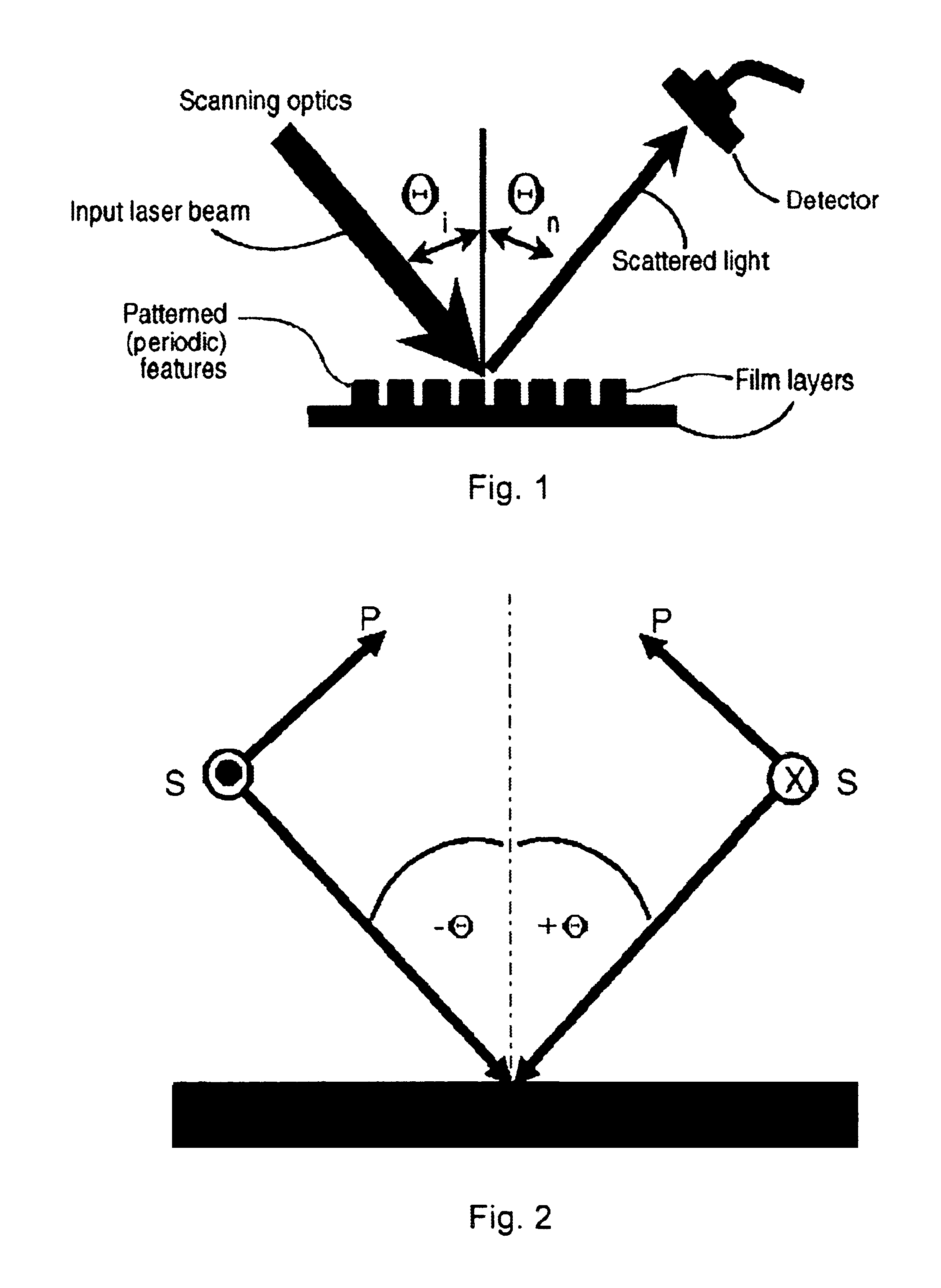
The raw signatures from this sample set showed a good deal of asymmetry. FIG. 6 depicts one signature from this data set with the positive and negative halves of the angular scan superimposed (‘mirrored’) on top of one another. Clearly, as the figure illustrates, the two halves are not the same. In fact, they differ at some angles by more than 5% in terms of reflectivity, and the structure of the signature differs at some angles as well. Because the measurements were made in the conical grating orientation, this is a sign of profile asymmetry.

The raw signatures from this data set matched well to the model. Sidewall angle results from these wafer measurements can be seen in FIG. 7. Recall that the library a...

example 2

Etched Poly-Si Lines

The linewidths for this sample set ranged from 150 to 300 nm. The stack was comprised of patterned (etched) poly-Si on oxide on Si substrate. The raw signatures from this sample set showed a slight amount of asymmetry when measured in the conical configuration. FIG. 8 depicts one such signature with both the positive and negative halves of the signature ‘mirrored’ to illustrate this asymmetry.

In order to draw comparisons, the wafer used for these scatterometry measurements was cross-sectioned and measured by a SEM to determine the sidewall angles of the lines. FIG. 9 shows the results of comparing the left and right sidewall angle measurements of the two technologies. As the figure illustrates, both tools are reporting some degree of sidewall asymmetry, with the left wall angle being generally smaller. Furthermore, the sidewall angle correlation between the two techniques is good and shows similar trending from site to site.

example 3

193 nm Photoresist Lines

The last sample set investigated was a single wafer of 193 nm photoresist lines printed on a BARC layer, a poly layer, an oxide layer and a silicon substrate. The nominal feature sizes on this wafer were 180 nm lines.

For this wafer, the signature data was only mildly asymmetric when measured in conical mode. FIG. 10 depicts the S and P polarizations for one of these signatures ‘mirrored’ back upon itself. In contrast to the signature asymmetries observed from the previous samples, this asymmetry was relatively weak.

The left and right wall angle data for one row from this wafer can be seen in FIG. 11. Included on the plots in this figure are measurements made on the same sites with an AFM. Both measurement technologies agree well in terms of the overall magnitude of the wall angles. The AFM data shows more asymmetric measurements but are generally consistent with the data from the scatterometer. A comparison of the CD measurements obtained by the scatterometer...


PUM

PropertyMeasurementUnit
anglesaaaaaaaaaa
wall anglesaaaaaaaaaa
wall angleaaaaaaaaaa

Abstract

A method of and apparatus for measuring line profile asymmetries in microelectronic devices comprising directing light at an array of microelectronic features of a microelectronic device, detecting light scattered back from the array comprising either or both of one or more angles of reflection and one or more wavelengths, and comparing one or more characteristics of the back-scattered light by examining data from complementary angles of reflection or performing a model comparison.

Description

BACKGROUND OF THE INVENTION1. Field of the Invention (Technical Field)The present invention relates to optical inspection of microelectronic devices, in particular measurement of line profile asymmetry using scatterometry.2. Background ArtNote that the following discussion refers to a number of publications by author(s) and year of publication, and that due to recent publication dates certain publications are not to be considered as prior art vis-a-vis the present invention. Discussion of such publications herein is given for more complete background and is not to be construed as an admission that such publications are prior art for patentability determination purposes.The fabrication of a microelectronic device is a complicated procedure that uses a variety of equipment for the different process steps involved. First, the lithography process transfers the image being made into a light sensitive material known as photoresist. This image in photoresist, in turn, acts as a mask for th...

Claims


Application Information

Patent Timeline
Patent Type & Authority Patents(United States)
IPC IPC(8): G01B11/00G03F7/20G01N21/956G01B11/24H01L21/027H01L21/66
CPCG01B11/00G01N21/95607G03F7/70633G03F7/70625G03F7/705G01B11/02
Inventor RAYMOND, CHRISTOPHER J.
Owner ONTO INNOVATION INC
Why Eureka
Try Eureka