Integrated circuit devices having high precision digital delay lines therein

a technology of integrated circuits and delay lines, which is applied in the direction of pulse manipulation, pulse technique, instruments, etc., can solve the problems of small delay per stage, insufficient noise suppression of separate power supply pins, and undesirable changes in the output timing of delay lines. , to achieve the effect of high resolution, low power consumption requirements, and excellent power supply

Inactive Publication Date: 2005-02-15
SK HYNIX INC
View PDF59 Cites 17 Cited by
  • Summary
  • Abstract
  • Description
  • Claims
  • Application Information

AI Technical Summary

Benefits of technology

[0006]Integrated circuit delay devices according to embodiments of the present invention have high resolution and excellent power supply and ground noise immunity. The delay devices may also be designed to have low power consumption requirements and low transistor count. In some embodiments, these delay devices include a digital delay line that is configured to provide a percent-of-clock period delay to a timing signal accepted at an enabled one of a plurality of injection ports thereof. The digital delay line may be responsive to an injection control signal having a value that sets a length of the delay by specifying a location of the enabled one of the plurality of injection ports, with the end of the delay line being a fixed output port.
[0007]A delay line control circuit is also provided that is responsive to a clock signal having a period from which the percent-of-clock period delay is preferably measured. This clock signal may be a highly accurate clock signal that is generated by a delay locked loop (DLL). The delay line control circuit is configured to generate the injection control signal by counting multiple cycles of a high frequency ring oscillator signal having a period less than, and typically substantially less than, the clock period, over a time interval having a duration greater than, and typically substantially greater than, the clock period. The ring oscillator signal may be generated by a ring oscillator having a relatively small number of stages and the time interval may be sufficiently long so that a large number of cycles of the ring oscillator signal may be counted over many periods of the clock signal. In this manner, a cycle count derived from the ring oscillator may be averaged over many periods of the clock signal. This makes the cycle count more stable and less sensitive to transient changes in the clock period. The cycle count is then evaluated to determine an appropriate delay to be provided by the digital delay line.
[0009]According to preferred aspects of these embodiments, the delay elements in the cascaded string each include a pair of PMOS load transistors having gate electrodes electrically coupled to a first bias signal line and current carrying terminals (e.g., drain terminals) electrically coupled to a power supply line. To enhance the noise immunity characteristics of the digital delay line, a first bias signal generator is provided to float the first bias signal line and the gate electrodes connected thereto at a first bias voltage when the digital delay line is active. The floating of the gate electrodes of the load transistors will support more constant gate-to-source voltages across the load transistors when noise is present on the power supply line. These more constant voltages, which are a consequence of capacitive coupling between each gate electrode and source terminal of a respective load transistor, provide more uniform I-V characteristics for the delay elements when the delay line is active. These more uniform I-V characteristics will necessarily translate into more uniform delay characteristics for each of the delay elements, notwithstanding the presence of power supply noise.
[0013]The delay line control circuit may also include a first multi-bit wide latch having data inputs that are electrically coupled to outputs of the counter. This first multi-bit wide latch may be responsive to a first “store” impulse that causes the latch to automatically load a count value generated by the counter in-sync with the first store pulse. This first store pulse may be generated by a second pulse generator. This second pulse generator may be configured to decode a second plurality of outputs of the divide-by-N clock generator and generate a short duration pulse when the ring oscillator is inactive and the count value generated by the counter is valid.

Problems solved by technology

For high resolution, a small delay per stage is typically required.
A delay line which exhibits minimal change in delay in the presence of power supply and ground noise is important because changes in delay that result from unpredictable noise may cause significant undesirable changes in the output timing of the delay line.
However, because an integrated circuit chip substrate is commonly one of the power supply nodes, and because this node is typically common with the noise generating circuitry on the chip and the delay line, the use of separate power supply pins may not provide sufficient noise suppression.

Method used


Image

  • Integrated circuit devices having high precision digital delay lines therein
  • Integrated circuit devices having high precision digital delay lines therein
  • Integrated circuit devices having high precision digital delay lines therein

Examples


third embodiment

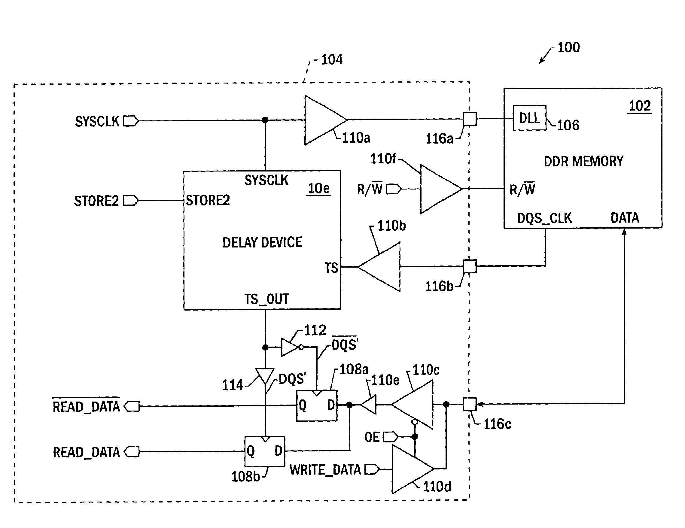
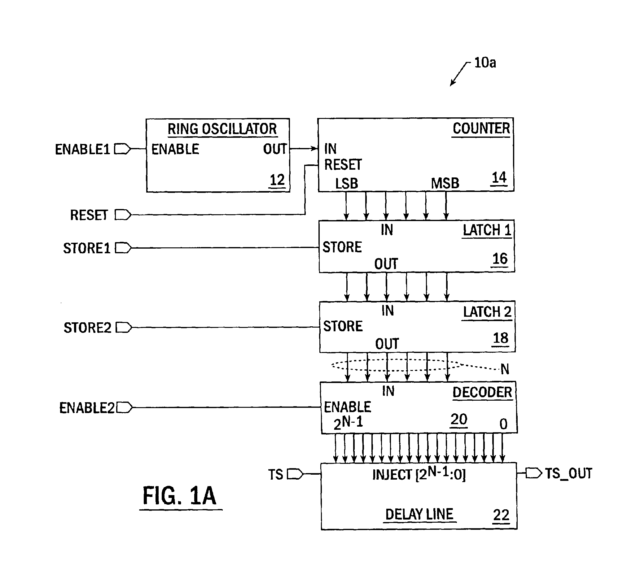
[0048]Referring now to FIG. 1C, an integrated circuit delay device 10c according to the present invention will be described. The delay device 10c of FIG. 1C is otherwise identical to the delay device 10b of FIG. 1B, however, the second latch 18 has been eliminated from the delay line control circuit (i.e., from between the first latch 16 and the decoder 20). Accordingly, in the delay device 10c of FIG. 1C, each automatic transfer of a count value from the counter 14 to the first latch 16 will automatically translate into an update of the injection control signal INJECT whenever the decoder 20 is enabled. This automatic update of the injection control signal INJECT will translate into an update in the location of the active injection port in the digital delay line 22 and a concomitant update in the delay provided by the digital delay line 22. This embodiment of FIG. 1C is typically less preferred than the embodiment of FIG. 1B, particularly in applications where the count value of th...

fourth embodiment

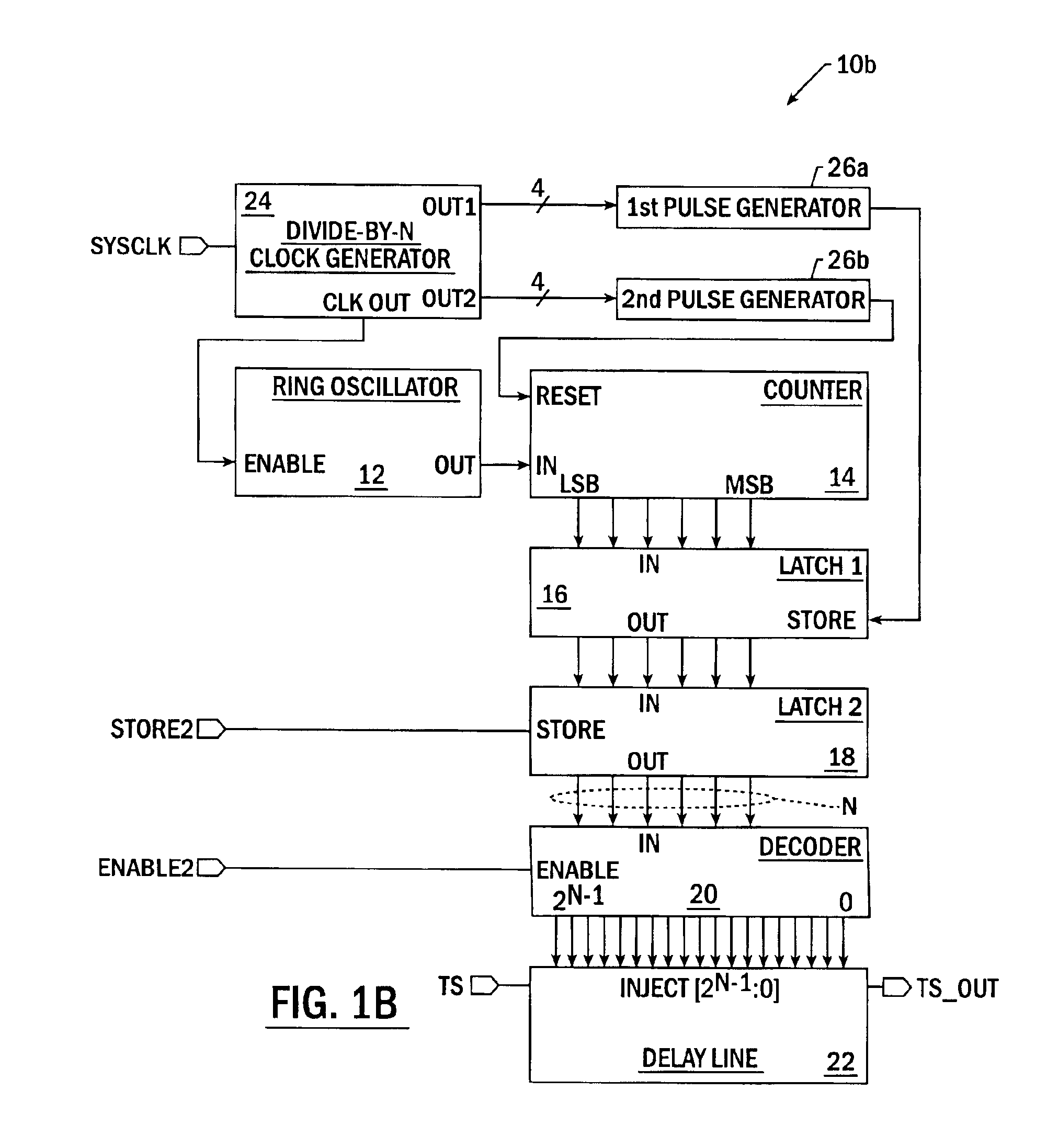
[0049]Referring now to FIG. 1D, an integrated circuit delay device 10d according to the present invention will be described. This delay device 10d is similar to the delay device 10b of FIG. 1B, however, a bias signal generator 30 is provided to improve the performance characteristics of the delay device 10d by making the delay provided by the digital delay line 22 less susceptible to power supply noise and / or sustained voltage level shifts on a power supply line that is electrically coupled to the delay device 10d. As illustrated, the bias signal generator 30 is responsive to two control signals. These two control signals include a bias strobe signal BIAS STROBE and a bias reset signal BIAS RESET. In response to these control signals, the bias signal generator 30 supplies the ring oscillator 12 and the digital delay line 22 with a pair of bias signals. These bias signals are illustrated as a PBIAS signal and an NBIAS signal. The ability of these bias signals to facilitate an improve...


PUM


Abstract

Integrated circuit delay devices include a digital delay line that is configured to provide a percent-of-clock period delay to a timing signal accepted at an enabled one of a plurality of injection ports thereof. The digital delay line may be responsive to an injection control signal having a value that sets a length of the delay by specifying a location of the enabled one of the plurality of injection ports, with the end of the delay line being a fixed output port. A delay line control circuit is also provided that is responsive to a clock signal having a period from which the percent-of-clock period delay is preferably measured. The delay line control circuit is configured to generate the injection control signal by counting multiple cycles of a high frequency ring oscillator signal having a period less than, and typically substantially less than, the clock period, over a time interval having a duration greater than, and typically substantially greater than, the clock period. The ring oscillator signal may be generated by a ring oscillator having a relatively small number of stages and the time interval may be sufficiently long so that a large number of cycles of the ring oscillator signal may be counted over many periods of the clock signal.

Description

CROSS-REFERENCE TO RELATED APPLICATION[0002]This application claims priority to U.S. Provisional Application Ser. No. 60 / 412,514, filed Sep. 20, 2002, the disclosure of which is hereby incorporated herein by reference.FIELD OF THE INVENTION[0003]The present invention relates to integrated circuit devices and, more particularly, to integrated circuit devices having digital delay lines therein.BACKGROUND OF THE INVENTION[0004]A delay line is often used to generate an output timing signal that is delayed a fixed fraction of a period of a clock signal after receipt of an input timing signal, which may, in some applications, be the clock signal. A delay line may use a fixed number of voltage controlled delay elements that are cascaded together into a string of delay elements. The delay associated with each delay element in a fixed-length string may be a function of an applied analog control voltage. Alternatively, a digital delay line may use a variable number of delay elements, with eac...

Claims


Application Information

Patent Timeline
Patent Type & Authority Patents(United States)
IPC IPC(8): G11C7/00H03H11/26H03K3/03H03K5/00H03K5/13H03K5/135H03L7/081
CPCH03H11/265H03K3/0322H03K5/133H03K5/135H03L7/0812H03K2005/00104H03K2005/00208H03K2005/00247H03K2005/00286H03K2005/00032
Inventor PROEBSTING, ROBERT J.TALLEDO, CESAR A.PILLING, DAVID J.
Owner SK HYNIX INC
Why Eureka
Try Eureka