Substrate processing system with positioning device and substrate positioning method
- Summary
- Abstract
- Description
- Claims
- Application Information
AI Technical Summary
Benefits of technology
Problems solved by technology
Method used
Image

Examples
Embodiment Construction
Preferred embodiments of the present invention will be described with reference to the accompanying drawings.
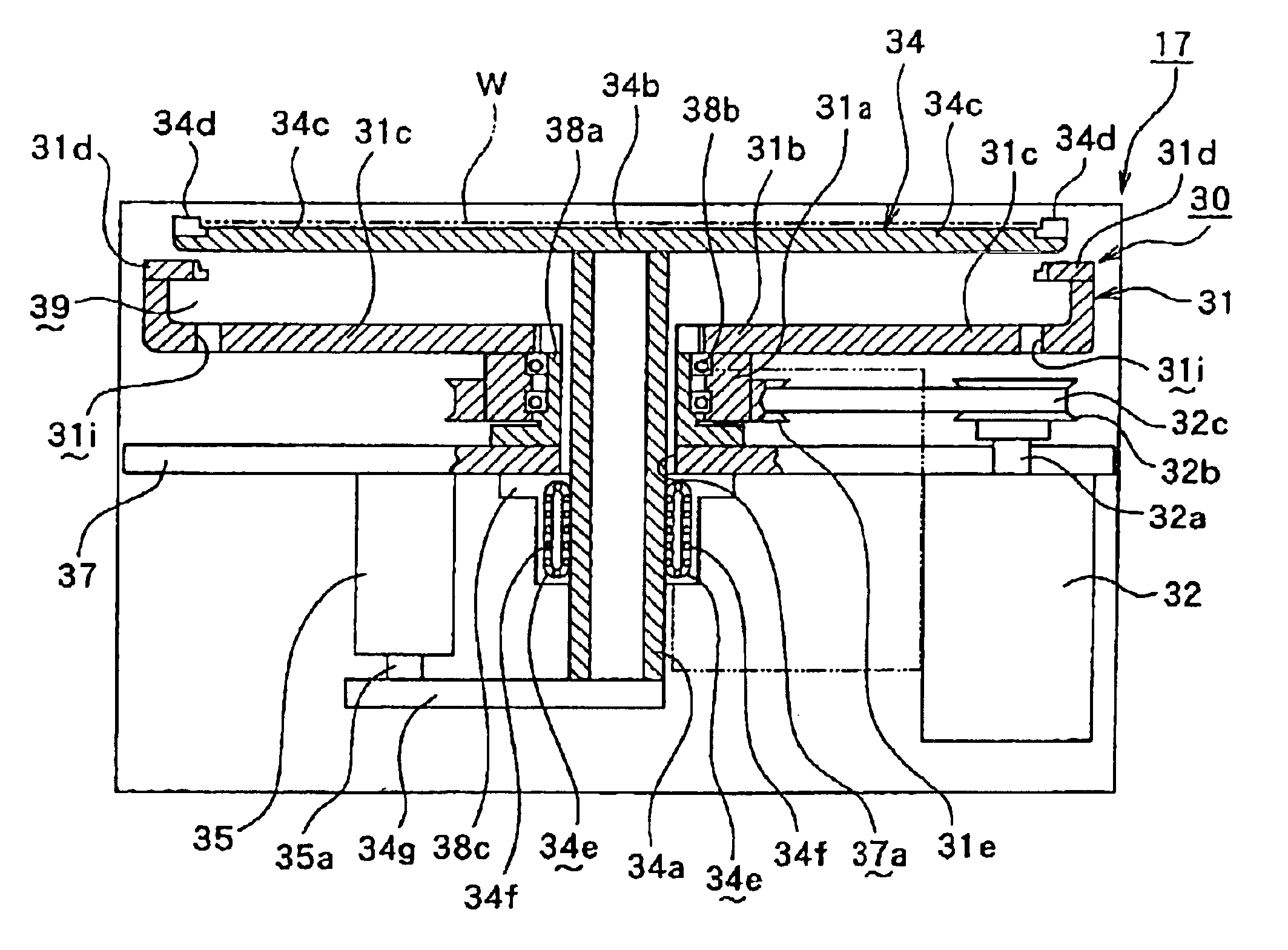
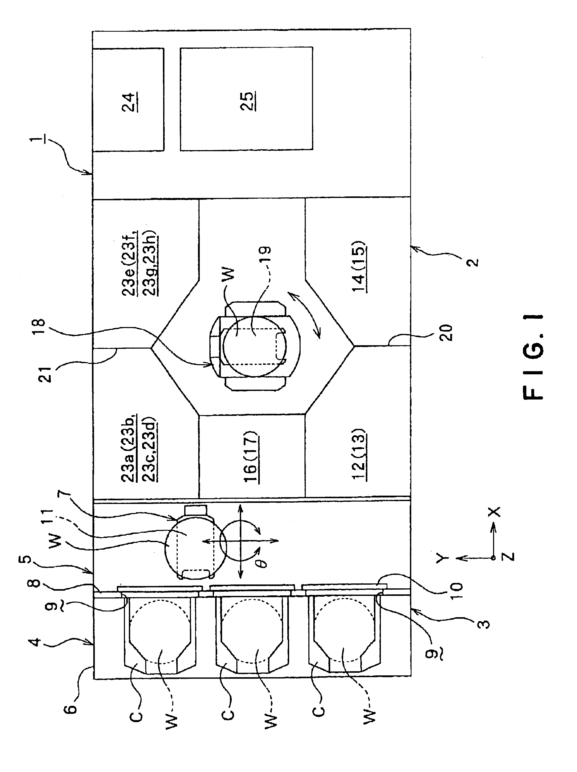
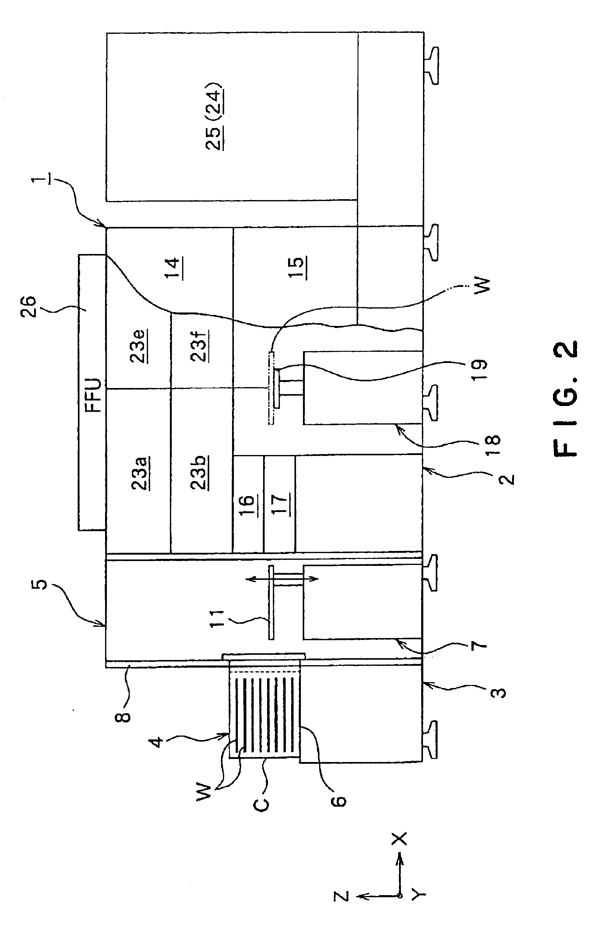
A substrate processing system 1 in a preferred embodiment according to the present invention will be described as applied to a substrate processing system for carrying out a resist film removing process for removing a resist film from the surface of a wafer and a cleaning process for cleaning the wafer. FIG. 1 is a schematic plan view of the substrate processing system 1 having a plurality of substrate processing units, and FIG. 2 is a schematic side elevation of the substrate processing system 1. The substrate processing system 1 includes, as principal components, a substrate processing section 2 for processing workpieces, such as semiconductor wafers W (hereinafter referred to simply as “wafers W”), and a receiving / delivering section 3 for receiving wafers W, carrying wafers W into the substrate processing section 2 and delivering processed wafers W.
The receiving / delivering...
PUM
 Abstract
Description
Claims
Application Information
 - Generate Ideas
- Intellectual Property
- Life Sciences
- Materials
- Tech Scout
- Unparalleled Data Quality
- Higher Quality Content
- 60% Fewer Hallucinations
Browse by: Latest US Patents, China's latest patents, Technical Efficacy Thesaurus, Application Domain, Technology Topic, Popular Technical Reports.
© 2025 PatSnap. All rights reserved.Legal|Privacy policy|Modern Slavery Act Transparency Statement|Sitemap|About US| Contact US: help@patsnap.com