Probe contact system using flexible printed circuit board

a flexible printed circuit board and contact system technology, applied in the direction of solid-state devices, instruments, semiconductor/solid-state device details, etc., can solve the problems of high cost, multi-layer ceramic substrates, and transformers b>50/b>, and achieve high reliability, long life in the contactor performance, and simple structure.

Inactive Publication Date: 2005-02-22
ADVANTEST CORP
View PDF11 Cites 36 Cited by
  • Summary
  • Abstract
  • Description
  • Claims
  • Application Information

AI Technical Summary

Benefits of technology

Therefore, it is an object of the present invention to provide a probe contact system to establish electrical connection with contact targets with a simple structure, low cost and high performance.
It is another object of the present invention to provide a probe contact system having a flexible printed circuit board, thereby eliminating the pogo-pin block, pogopins, coaxial cables, probe card and space transformer in the conventional technology.
According to the present invention, the probe contact system has a simple structure by eliminating many components used in the conventional technology. Namely, by incorporating the flexible printed circuit board, the probe contact system of the present invention is established without using the pogo-pin block, pogo-pins, coaxial cables, probe card and space transformer in the conventional technology. The flexible printed circuit board has signal patterns and works as a space transformer by changing pitches of the contactors to the pitches of the socket in the test head. The flexible printed circuit board works as signal cables for connecting the contactors with the test head, thereby obviating the probe card, pogo-pins and coaxial cables in the conventional technology.
The probe contact system of the present invention has a broad bandwidth covering high frequency region to meet the test requirements of next generation semiconductor technology. Since a large number of contactors are produced at the same time on a substrate trough a semiconductor production process, it is possible to achieve consistent quality, high reliability and long life in the contactor performance as well as low cost. Further, according to the present invention, the production process is able to produce a large number of contactors in a horizontal direction on the silicon substrate by using relatively simple technique. Such contactors are mounted on a contactor carrier in a vertical direction. The probe contact system in the present invention is low cost, and has high efficiency, high mechanical strength and reliability.

Problems solved by technology

The space transformer 50 has many signal patterns and is made of, for example, multi-layers of ceramic substrate, and is costly.
In the foregoing conventional example, to establish electrical connection with the contact pads of the semiconductor wafer, the probe contact system having many components has to be used, resulting in high cost.

Method used


Image

  • Probe contact system using flexible printed circuit board
  • Probe contact system using flexible printed circuit board
  • Probe contact system using flexible printed circuit board

Examples


Embodiment Construction

Examples of probe contact system of the present invention and examples of contactors for use in the probe contact system will be described with reference to FIGS. 4-13N. Although the present invention will be described for the case of testing a semiconductor wafer, the contact structure of the present invention can be used in testing LSI and VLSI chips, printed circuit boards and the like, or burning-in the semiconductor wafers and chips.

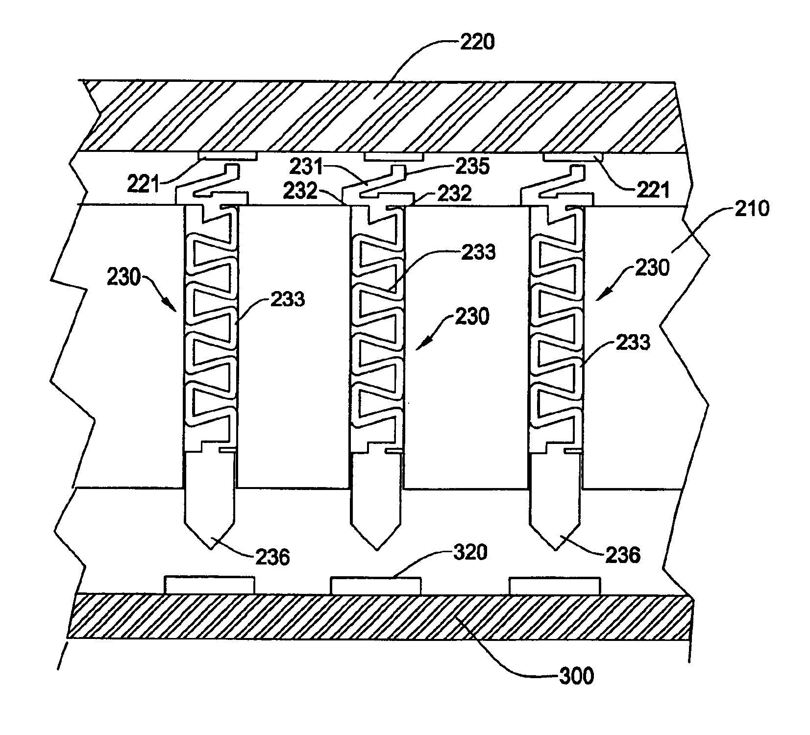
FIG. 4 is a cross sectional view of the probe contact system using the present invention. The test head 100 of the semiconductor test system is illustrated over the probe contact system. The probe contact system of FIG. 4 includes a main frame 201, a contactor carrier 210 mounted on a hollow portion of the main frame 201, a frame adaptor 202 for mounting the contactor carrier 210, and a flexible printed circuit board 220. A plurality of contactors 230 are mounted on the contactor carrier 210.

In this example, the probe contact system has a structure ...


PUM


Abstract

A probe contact system for establishing electrical connection with contact targets. The probe contact system is formed of a main frame, a flexible printed circuit board (PCB), a contactor carrier and a plurality of contactors. The flexible PCB has contact pads at a center area thereof and signal lines connected to the contact pads and extended to an end of the flexible PCB. The end of the flexible PCB with the signal lines is connected to a test head of a semiconductor test system. In one aspect, the contactor has a top spring to resiliently contact with the contact pads on the flexible PCB. In another aspect, the probe contact system includes a conductive elastomer sheet between the contactor and the flexible PCB thereby obviating the top spring of the contactor.

Description

FIELD OF THE INVENTIONThis invention relates to a contact structure to establish electrical connection with contact targets such as contact pads on semiconductor devices, and more particularly, to a probe contact system using a flexible printed circuit board and a plurality of contactors mounted on a contactor carrier for testing semiconductor devices with high speed, high density and low cost.BACKGROUND OF THE INVENTIONIn testing high density and high speed electrical devices such as LSI and VLSI circuits, a high performance probe contact system has to be used. The probe contact system typically includes a contact substrate (space transformer) having a large number of contactors or probe elements, a probe card for mounting the contact substrate, and a plurality of pogo-pins for connecting between the probe card and a test head of a semiconductor test system. The probe contact system interfaces between the test head of the semiconductor test system and semiconductor devices to test ...

Claims


Application Information

Patent Timeline
Patent Type & Authority Patents(United States)
IPC IPC(8): G01R1/067G01R1/073G01R3/00
CPCG01R1/06716G01R1/07314G01R3/00
Inventor ZHOU, YUYU, DAVID
Owner ADVANTEST CORP
Why Eureka
Try Eureka