Fail number detecting circuit of flash memory

a technology of failure number and detection circuit, which is applied in the field of semiconductor memory devices, can solve the problems of long acquisition time, long time consumption, and failure data that fails continuously in defective column sections

Inactive Publication Date: 2005-02-22
TOSHIBA MEMORY CORP
View PDF22 Cites 33 Cited by
  • Summary
  • Abstract
  • Description
  • Claims
  • Application Information

AI Technical Summary

Problems solved by technology

However, in the case of the first method, it takes a long time to acquire the result, and in the case of the second method, only information that all of the columns in the page have passed can be acquired.
This is because a defective column section continuously holds fail data in some cases.
In this case, it is possible to detect a preset number of fails by use of the first method, but it is required to serially read out data after the verify readout operation from all of the registers in the page and there occurs a problem that it takes a long time.

Method used


Image

  • Fail number detecting circuit of flash memory
  • Fail number detecting circuit of flash memory
  • Fail number detecting circuit of flash memory

Examples


second embodiment

[Second Embodiment]

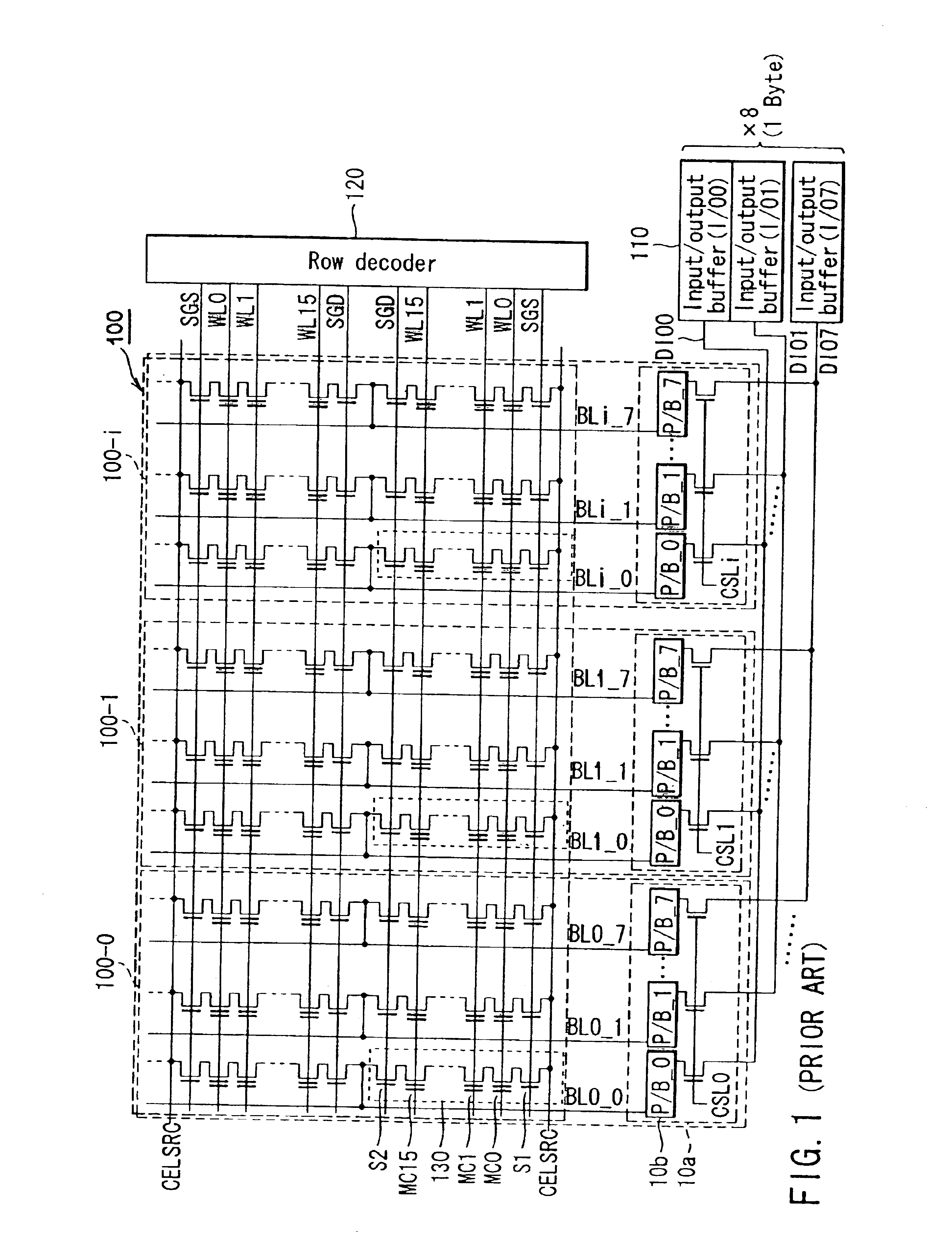
In the first embodiment described above, a case wherein the number of columns each containing fail data or a register (page buffer) P / B having “1” data on the node n2 of the latch circuit is detected is explained, but if the register group 10a of each column is replaced by a circuit having a configuration as shown in FIG. 9, the number of fail data items or registers P / B each having “1” data on the node n2 of the latch circuit can be detected irrespective of the column unit.

That is, in the circuit shown in FIG. 9, different signals VFY0 to VFY7 are supplied to the gates of NMOS transistors 29 of the respective registers 10b.

Next, the operation of the circuit shown in FIG. 9 is explained with reference to FIGS. 10A, 10B and 11. In FIGS. 10A and 10B, numerals in the P / B group 10a of each column express data items (“1” indicates “fail” and “0” indicates “pass”) which the registers P / B_0 to P / B_7 hold.

First, as shown in FIG. 10A, the signal VFY0 is set to the “H” lev...

first embodiment

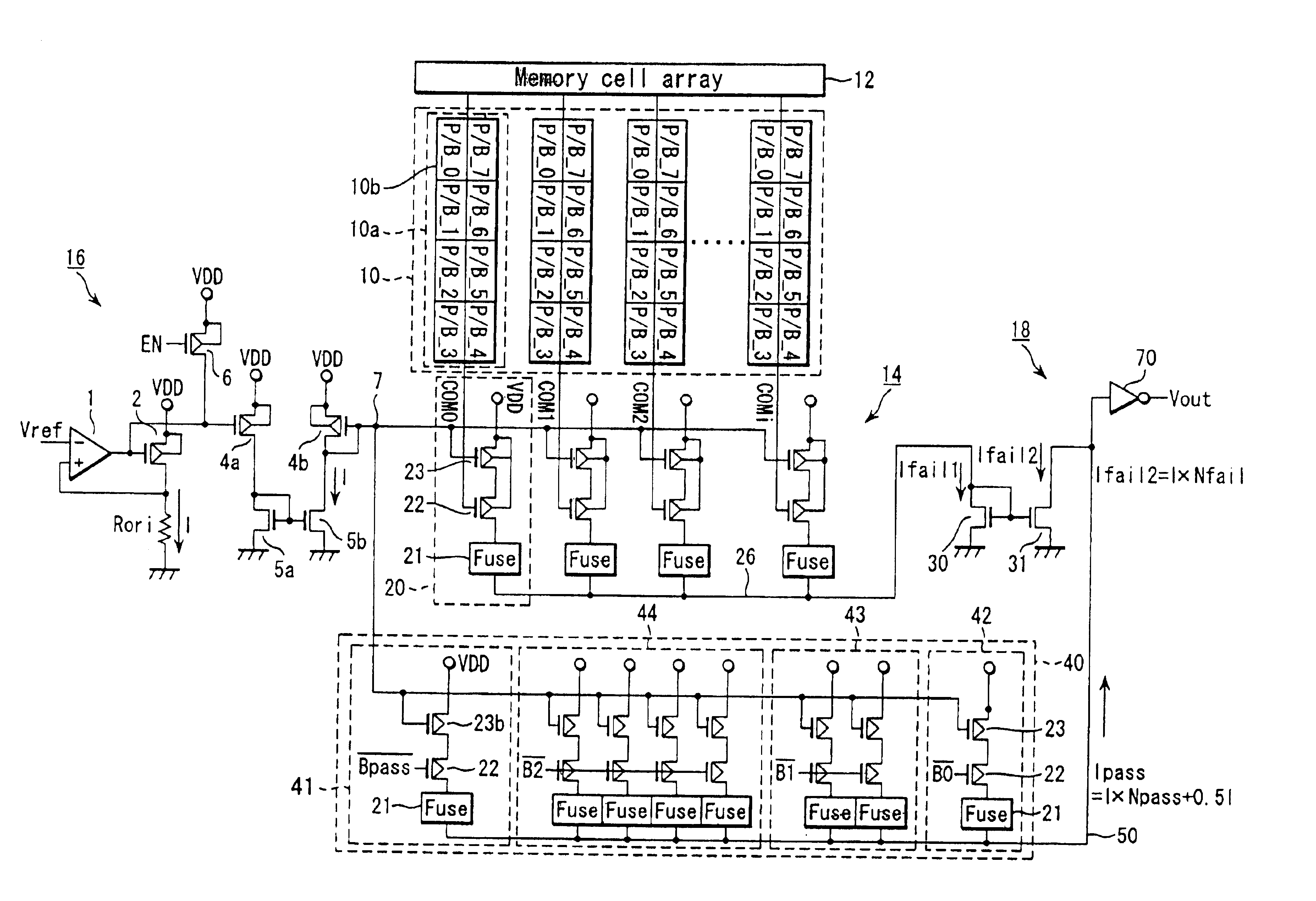
The first embodiment relates to the column redundancy, but the second embodiment relates to an error code correction function (ECC). That is, it is assumed that program fails of several bits can be permitted by the ability of the error code correction function of the system using the semiconductor memory. If verify fails of several bits are permitted in the program operation, an operation which detects the number of thus failed bits is effective and can be performed at higher speed in comparison with the conventional case.

third embodiment

[Third Embodiment]

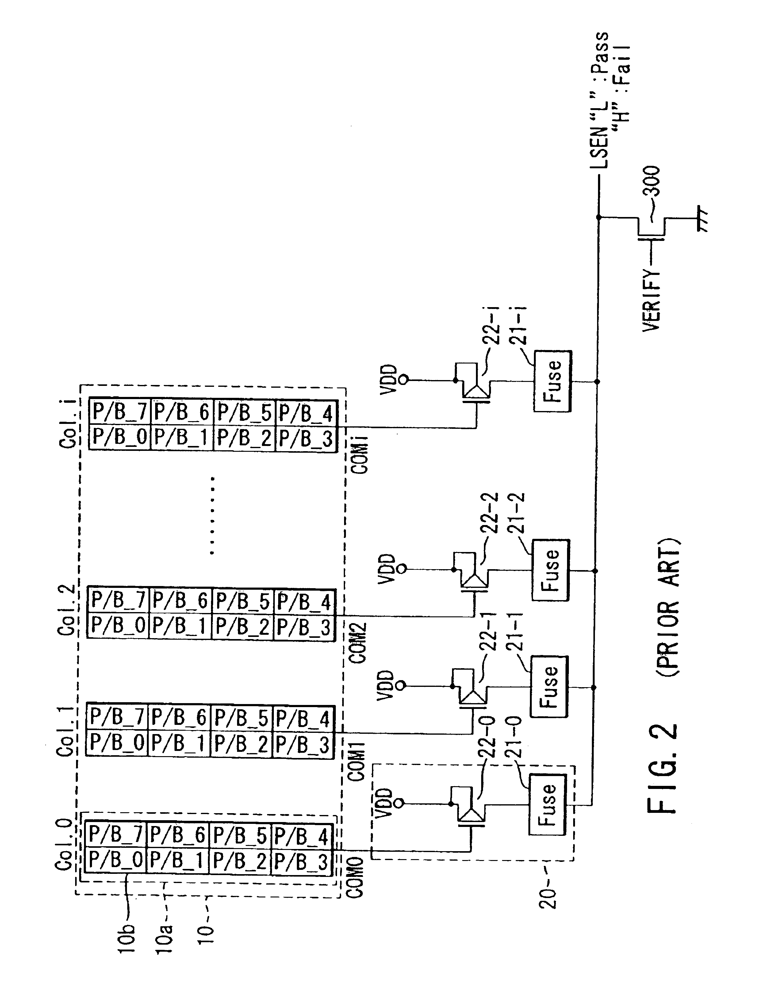
FIG. 12 illustrates a semiconductor memory device according to a third embodiment of this invention and shows a modification of the construction of the circuit shown in FIG. 3. In FIG. 12, portions which are the same as those of FIG. 3 are denoted by the same reference numerals and the detail explanation thereof is omitted.

In the first embodiment shown in FIG. 3, the constant current flowing in each of the columns is determined by the PMOS transistor 23, but in the third embodiment shown in FIG. 12, it is determined by use of an NMOS transistor 23c.

A portion which determines the current I is the same as in the circuit portion of FIG. 3, but a current of 0.5I is generated by use of a PMOS transistor 4c and the gate potential of a diode-connected NMOS transistor 5c is input to a permissible fail number setting circuit 40. Further, the construction is made to cause a current I to flow in a PMOS transistor 4d and cause the current I to flow in a current passage circui...


PUM


Abstract

A semiconductor device includes a memory cell array, latch circuits, first to third circuits and a current control circuit. The memory cell array includes NAND cells arranged therein. The latch circuits temporarily hold data read out from the memory cell array. The first circuit generates a first current varying in proportion to “1” or “0” of binary logic data of one end of the plurality of latch circuits. The second circuit generates a second current which is preset. The third circuit compares the first current with the second current. The value of “1” or “0” of binary logic data of the one end of the plurality of latch circuits is detected based on a result of the comparison between the first current and the second current.

Description

BACKGROUND OF THE INVENTION1. Field of the InventionThis invention relates to a semiconductor memory device such as a flash memory and more particularly to a method which is used for detecting the result of verify readout in the programming operation and erase operation and is adequately applied to a flash memory having a large batch processing unit.2. Description of the Related ArtIn a flash memory, the effective programming speed and erase speed are enhanced by programming data in the unit of page and performing the erase operation in the unit of page or in the unit of plural pages. In the programming operation in the page unit, a program pulse applying operation and verify readout operation are performed after program data is serially input and data is input to registers of one page, and then the program pulse applying operation and verify readout operation are repeatedly performed until whole data of the page is programmed. At this time, two methods are conventionally used to de...

Claims


Application Information

Patent Timeline
Patent Type & Authority Patents(United States)
IPC IPC(8): G11C16/34G11C16/06G11C16/04G11C16/02G11C29/04G11C29/12
CPCG11C16/3436G11C16/3459G11C16/3445G11C16/06
Inventor HOSONO, KOJIIKEHASHI, TAMIOTANAKA, TOMOHARUIMAMIYA, KENICHINAKAMURA, HIROSHITAKEUCHI, KEN
Owner TOSHIBA MEMORY CORP
Why Eureka
Try Eureka