
Apparatus for and method of heat treatment by light irradiation

a technology of light irradiation and apparatus, applied in lighting and heating apparatus, muffle furnaces, furnaces, etc., can solve the problems of semiconductor wafers that may break, semiconductor wafers that are easy to break, and more ions than required to be implanted, so as to prevent a substrate from breaking

Active Publication Date: 2005-02-22
DAINIPPON SCREEN MTG CO LTD
View PDF11 Cites 40 Cited by
  • Summary
  • Abstract
  • Description
  • Claims
  • Application Information

AI Technical Summary

Benefits of technology

The substrate in a floating state can freely move at the time of flashlight irradiation. As a result, even when instantaneous flashlight irradiation causes rapid thermal expansion of the substrate surface, the substrate does not suffer a great stress. This can prevent the substrate from breaking at the time of heat treatment.
It is therefore an object of the present invention to provide a heat treatment apparatus and heat treatment method which is capable of preventing a substrate from breaking during heat treatment.

Problems solved by technology

When such a phenomenon takes place, implanted ions are diffused even if a high concentration of ions are implanted into the surface of the semiconductor wafer, resulting in a problem in that more ions than required need to be implanted.
When energy of irradiated light exceeds a threshold value, rapid thermal expansion at the surface may cause the semiconductor wafer to break with a high probability.
However, when heating a semiconductor wafer being held by a susceptor by irradiating a flashlight from a xenon flash lamp, the semiconductor wafer may break even with a flashlight having energy lower than the above threshold value.
This is because, when the semiconductor wafer is going to warp to be convex due to rapid thermal expansion at the surface resulting from instantaneous flashlight irradiation, a great force is applied to a contact part, if any, between an end of the wafer and a pocket edge of the susceptor or positioning pin, whereas there is not sufficient time for the wafer to move sliding over the susceptor in order to relieve such stress.
As a result, even when irradiating a flashlight having energy lower than the above-mentioned threshold value, stress generated at a contact part, if any, between an end of the semiconductor wafer and something at the time of instantaneous thermal expansion causes the semiconductor wafer to break.

Method used


Image

  • Apparatus for and method of heat treatment by light irradiation
  • Apparatus for and method of heat treatment by light irradiation
  • Apparatus for and method of heat treatment by light irradiation

Examples


first preferred embodiment

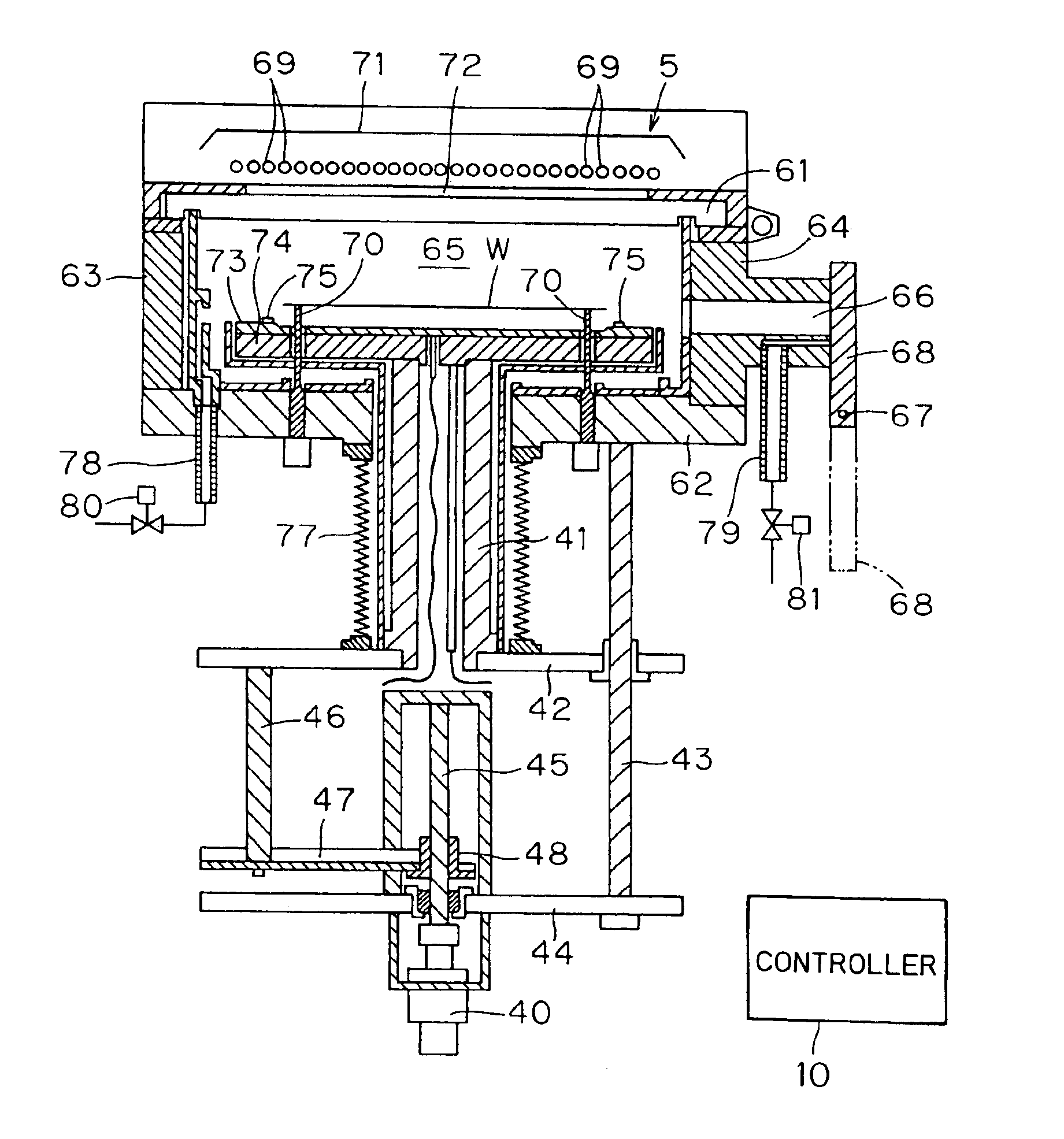
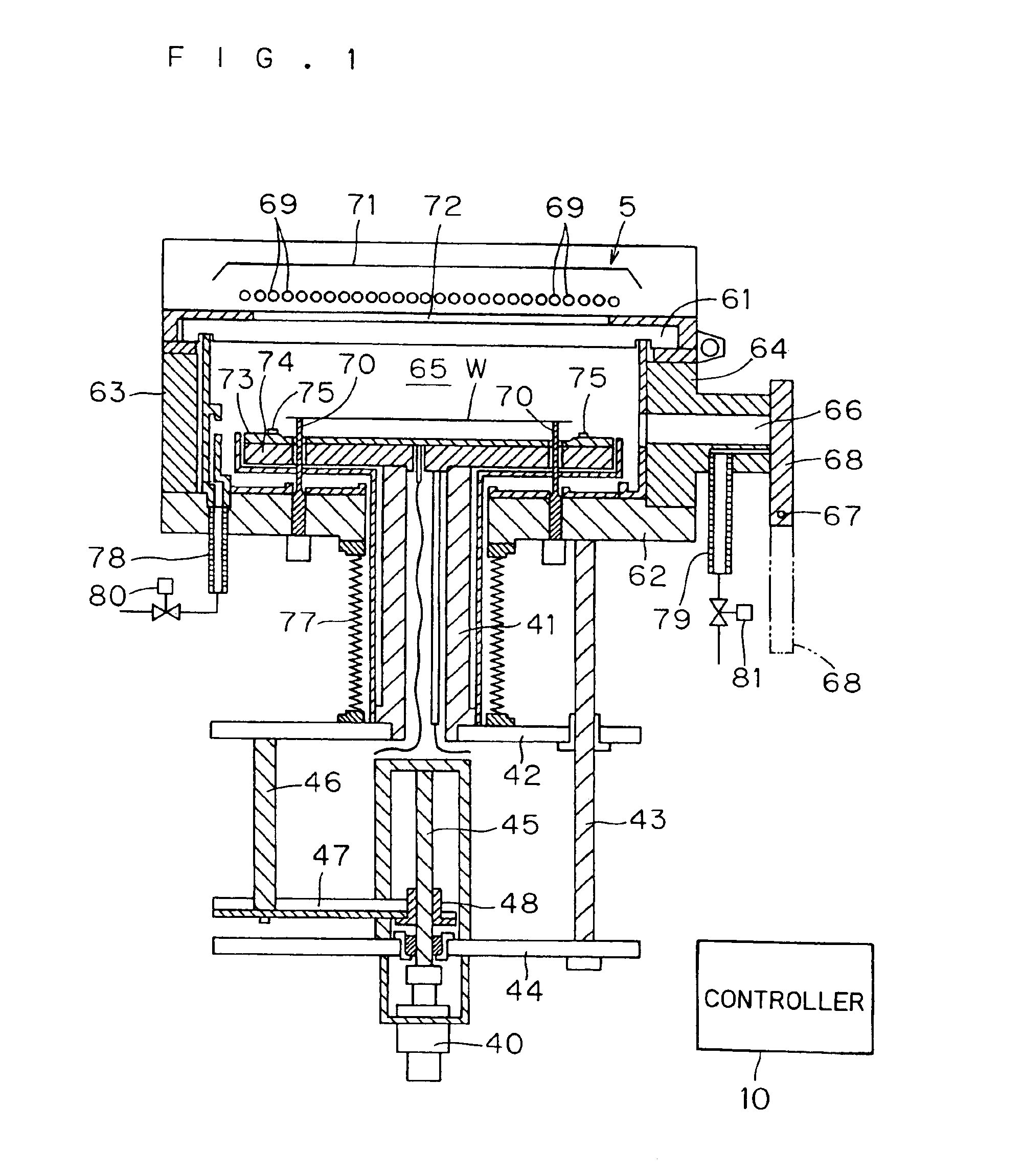
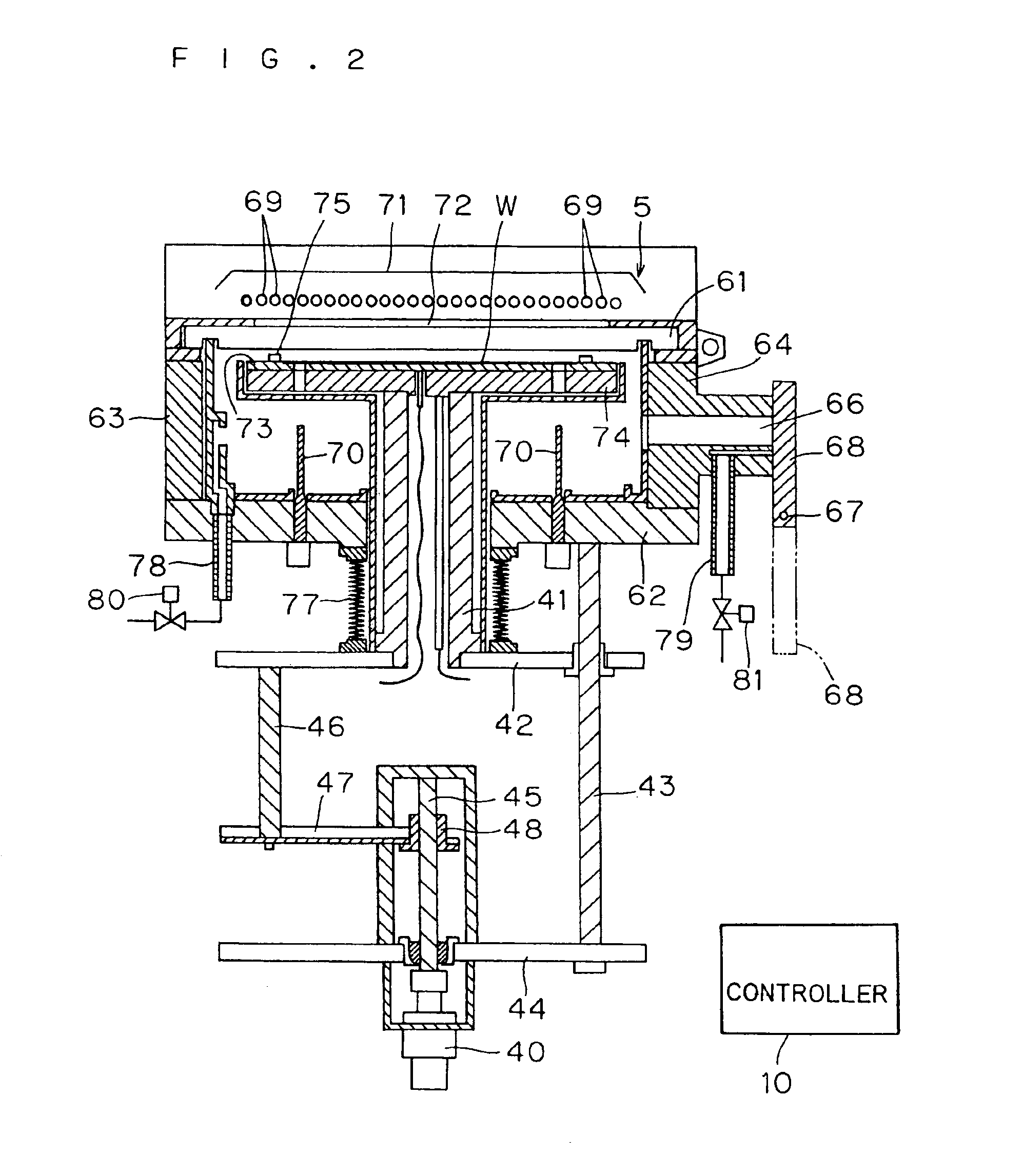
FIGS. 1 and 2 are sectional side elevations each illustrating the structure of a heat treatment apparatus according to a first preferred embodiment of the present invention. This heat treatment apparatus is intended to perform heat treatment on a substrate such as a circular semiconductor wafer by a flashlight emitted from a xenon flash lamp.

The heat treatment apparatus includes a chamber 65 formed by a light transmitting plate 61, a bottom plate 62 and a pair of side plates 63 and 64 and intended for housing a semiconductor wafer W therein and performing heat treatment on the semiconductor wafer W. The light transmitting plate 61 forming the upper portion of the chamber 65 is made of, for example, an infrared transmissive material such as quartz, and functions as a chamber window for transmitting light emitted from a light source 5 to guide it into the chamber 65. The bottom plate 62 of the chamber 65 has support pins 70 provided in a standing manner and extending through a suscept...

second preferred embodiment

Next, a second preferred embodiment of the present invention will be described. A heat treatment apparatus according to the present embodiment has exactly the same structure as that of the first preferred embodiment, explanation of which is thus omitted here. The present embodiment differs from the first preferred embodiment only in the procedure of heat treatment operation performed on the semiconductor wafer W.

FIG. 6 is a flow chart illustrating the procedure of heat treatment operation according to the second preferred embodiment. In the present embodiment, the semiconductor wafer W is transported into the chamber 65 by a transport robot not shown through the opening 66 and is mounted on the support pins 70 while the susceptor 73 and heating plate 74 are located at the transporting position of the semiconductor wafer W shown in FIG. 1 (step S1). Upon completion of transport of the semiconductor wafer W, the opening 66 is closed by the gate valve 68. Thereafter, the susceptor 73 a...

third preferred embodiment

Next, a third preferred embodiment of the present invention will be described. A heat treatment apparatus according to the present embodiment has the same structure as that of the first preferred embodiment except for an additional mechanism for discharging nitrogen gas from the upper surface of the susceptor 73 toward the lower surface of the semiconductor wafer W. FIG. 7 is a sectional side elevation illustrating the structure of the heat treatment apparatus according to the third preferred embodiment.

In the heat treatment apparatus of the present embodiment, a gas supply pipe 90 is provided in the susceptor 73 and heating plate 74 so as to hang down therefrom. The gas supply pipe 90 has its top end inserted into the susceptor 73 and heating plate 74 to form a discharge port 93 on the upper surface of the susceptor 73. The discharge port 93 is directed toward the lower surface of the semiconductor wafer W.

The gas supply pipe 90 has its base end communicating with a gas pipe 91. Th...


PUM

PropertyMeasurementUnit
temperaturesaaaaaaaaaa
temperature T1aaaaaaaaaa

Abstract

A semiconductor wafer is held by support pins horizontally. A susceptor and a heating plate are moved upwardly so that the semiconductor wafer is transferred from the support pins to the susceptor. At this time, a gas layer is sandwiched between the upper surface of the susceptor and the lower surface of the semiconductor wafer to cause the semiconductor wafer to float over the upper surface of the susceptor for about seventy seconds immediately after the semiconductor wafer is mounted on the upper surface of the susceptor. Then, flash lamps are lit up to perform flash heating while the semiconductor wafer is floating over the upper surface of the susceptor. Even when flashlight irradiation causes rapid thermal expansion of the wafer surface, the semiconductor wafer does not suffer a great stress. This can prevent the semiconductor wafer from breaking.

Description

BACKGROUND OF THE INVENTION1. Field of the InventionThe present invention relates to a heat treatment apparatus and method of performing heat treatment on a substrate by irradiating a flashlight onto a semiconductor wafer, a glass substrate or the like (hereinafter briefly referred to as a “substrate”).2. Description of the Background ArtIn an ion activation step for an ion-implanted semiconductor wafer, a heat treatment apparatus such as a lamp annealing apparatus with a halogen lamp employed therein has conventionally been used. Such a heat treatment apparatus heats (anneals) a semiconductor wafer to temperatures ranging, for example, between about 1000 and 1100° C. thereby achieving ion activation in the semiconductor wafer. In such a heat treatment apparatus, the temperature of a substrate is raised at a speed of about several hundred degrees per second by the use of energy of light emitted from the halogen lamp.However, it has been found out that, in the case of achieving ion a...

Claims


Application Information

Patent Timeline
Patent Type & Authority Patents(United States)
IPC IPC(8): H01L21/00H05B3/00H01L21/324
CPCH05B3/0047H01L21/67115H01L21/324
Inventor KUSUDA, TATSUFUMIUEYAMA, TSUTOMU
Owner DAINIPPON SCREEN MTG CO LTD
Learn More